Design of shutdown function for boost converter
Time:2022-07-09
Views:2015
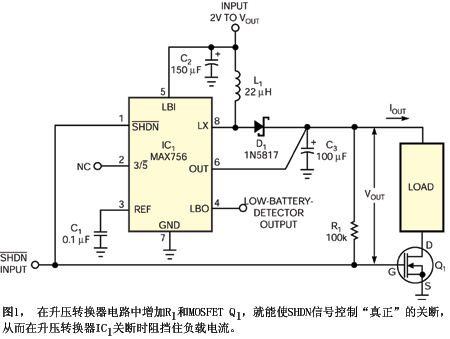
Figure 1 shows the boost switch converter circuit, which has a well-known problem: if the input of boost converter IC1 is pulled down to turn off the boost converter, the external inductance L1 and forward biased Schottky diode D1 can make the load continue to draw current. For battery powered equipment, this is a heavy load (300 MA). This useless DC current path may quickly drain the battery. Adding an n-channel MOSFET Q1 and a 100 K resistor R1 can break the useless current path in case of power failure, so as to solve this problem. Such a circuit is suitable for the application of battery powered system in which the microcontroller deals with the problem of power management.

Applying a logic low level at the input can simultaneously turn off the switch converter max756 and turn off the MOSFET, so the load current is blocked by removing the ground connection of the load. When the signal is removed, the 100 K Ω pull-up resistor will raise the MOSFET gate potential, making the MOSFET turn on. As the grounding is reconnected, the load can obtain current from the working boost conversion circuit.
In order to obtain the best results under large load current, a logic low-level MOSFET with an appropriately low on resistance should be selected for Q1. The drain source breakdown voltage of MOSFET shall also be able to withstand at least twice the maximum output voltage from the boost converter. If necessary, more than two MOSFETs can be connected in parallel to reduce the effective on resistance of Mosfets.
|
Disclaimer: This article is transferred from other platforms and does not represent the views and positions of this site. If there is infringement or objection, please contact us to delete. thank you! |


