Class D amplifier design challenges for optimal audio performance
Time:2022-07-20
Views:1980
Abstract: Class D amplifier has gradually become the preferred topology for high-end household a/v devices and mobile devices, which can help designers realize the combination of high performance and small size, which is what users all over the world expect and need. Now, the emergence of highly integrated class D amplifier devices, including the entire amplifier module in a single package, enables enterprises to bring new products with highly competitive prices to the market faster, and their audio performance reaches or exceeds that of traditional analog amplifiers.
Class D amplifier has gradually become the preferred topology for high-end household a/v devices and mobile devices, which can help designers realize the combination of high performance and small size, which is what users all over the world expect and need. Now, the emergence of highly integrated class D amplifier devices, including the entire amplifier module in a single package, enables enterprises to bring new products with highly competitive prices to the market faster, and their audio performance reaches or exceeds that of traditional analog amplifiers.
Class D audio amplifier can operate at an efficiency level of about 90%, allowing designers to provide extremely high audio output with or without a small radiator. In this way, new small audio products can be realized, which cannot be achieved by using traditional analog class AB amplifier.
However, it is not easy to design class D amplifier from scratch. The great challenge is to ensure that the amplifier can operate safely. However, if this can be achieved, the audio performance is more or less predictable and mainly depends on the quality of the components used.
This paper will compare the design and performance of class AB and class D amplifiers, introduce the main challenges related to class D design, and explain how higher integration can help engineers complete the design and achieve cost and performance goals faster.
Analog and digital amplifier design
For many years, class AB analog topologies have been widely used in the entire audio industry. Class AB operation combines class a operation (in which the output transistor will never be turned off, resulting in high power consumption) and class B operation (in which each device will only be turned on for half a signal cycle (180 degrees), thus greatly reducing power consumption). In class AB amplifiers, each output device will be turned on about 200 degrees, sacrificing a certain amount of energy efficiency, but a small amount of overlap is generated, which reduces the crossover distortion when one device is turned off and the other is turned on. In order to achieve the highest possible audio fidelity with class AB amplifiers, the designer must bias the transistors in an optimal way in order to maintain operation in the linear region and minimize crossover distortion. Device selection and circuit layout will also affect the quality and type of sound, so that designers can optimize it for some applications and environments. Generally, the working efficiency of class AB amplifier is 30-35%. This is much higher than the 15-30% efficiency of pure class a design, but large radiators need to be added, which increases the cost and volume of finished products.
In the past, equipment buyers were easy to accept the problem of large volume of advanced high fidelity audio and audio / video equipment. However, today‘s demand for high-performance mobile devices and more popular ultra-thin home multimedia systems increasingly requires digital amplifiers that can provide the same or higher sound quality, occupy less PCB area, work more efficiently, consume less energy, and require fewer radiators.
In class D amplifiers, the output transistors operate in the switching mode, rather than in the linear region, so that designers can provide products with smaller shape and higher energy efficiency expected by end users today. At the output end, a low-pass filter is used to remove the switching carrier signal and its harmonics, so as to produce a high-quality amplified audio signal.
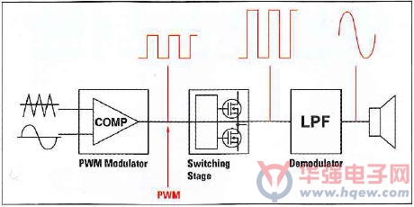
The general function module of class D amplifier is shown in Figure 1. The input audio signal is compared with the high-frequency sawtooth waveform to generate the input pulse width modulation square wave expression. The sawtooth frequency is usually around 400kHz. This is just outside the frequency range of the audio signal, so it helps to simplify the design of the output filter.

Figure 1: main functional modules of class D amplifier.
Then, the pulse width modulation equivalent signal of the audio signal is used to drive the amplifier output stage, which is a full bridge or half bridge MOSFET array. Output topology selection depends on system requirements, such as cost, power output, and power supply design. For example, the half bridge output stage needs positive and negative power supply. On the other hand, the full bridge can be powered by a single power supply, and can also produce a higher output for a given power supply voltage.
In both cases, the characteristics of the output MOSFET are optimized for class D audio amplifier operation to maximize efficiency and ensure low total harmonic distortion + noise (thd+ n) and EMI. This requires low on resistance (for achieving high power density in the end product) and optimized gate charge and volume diode reverse recovery characteristics (for fast and efficient switching).
The amplified audio signal is contained in the square wave at the output of the MOSFET bridge. Low pass filtering eliminates the external frequency of audio and restores the pure audio signal to drive the speaker.
Class D design challenge
Because the power transistor is either in the hard on state or in the full off state, the designer can optimize the performance without any adjustment. However, the PWM conversion stage must be well protected, and requires accurate grid control and low pulse width distortion, as well as high and low-end drive signals to match, in order to minimize the dead time and achieve the best linearity.
The development risk is very high. The design of class D amplifier is originally a power electronics challenge, which requires knowledge of switch control and protection circuit design. If these problems are not solved correctly in the design phase, the prototype may not run or suffer catastrophic failures during testing. If such failures occur, it will be very difficult to identify and correct these defects, which will also increase costs and delay the completion of the project.
Referring to figure 1, we can identify the main design challenges related to the main functional modules of the amplifier.
Referring to figure 1, we can identify the main design challenges related to the main functional modules of the amplifier.
The main quality factors of audio amplifier are noise and total harmonic distortion (THD). In class D amplifiers, these are caused by defects, including limited switching time, overshoot / undershoot, and power fluctuations. To minimize these effects, we need to carefully design an appropriate error amplifier, which can correct the defects in the output stage by comparing the input and output audio signals. However, the typical error amplifier used in class A or AB design is not suitable for the noisy environment of class D audio amplifier. It may be difficult and expensive to purchase a suitable operational amplifier and ensure high enough noise immunity.
In terms of noise isolation, class D topology requires that the front and back ends should be as close to each other as possible. In a discrete solution, the designer must decide how to isolate the noise sensitive analog circuit at the input from the potentially damaging switching noise generated at the output stage. The integrated class D amplifier module allows designers to bypass these challenges. However, it is important to realize sufficient electrical isolation between the two circuits by using appropriate devices.
PWM comparator and level shift
After the error amplifier processes the input audio signal and generates an appropriately shaped output, the comparator will convert the analog signal into a pulse width modulation (PWM) signal.
Gate drive and MOSFET switch
The gate drive stage receives the PWM signal from the comparator. At this stage, a dead time is inserted between the conduction phases of the high-end and low-end MOSFETs to prevent excessive current from flowing through the bridge. The dead time eliminates the influence of the output MOSFET switch delay time, which will cause destructive through current passage, so it can ensure safe operation. However, inserting dead time can also lead to nonlinearity, resulting in unnecessary distortion.
Accurate grid control is the key to achieve high audio performance. The gate driver must have the characteristics of low pulse width distortion, and the high-end and low-end gate driver stages must be matched. These two characteristics are essential to minimize dead time in order to achieve linear amplifier performance. In fact, dead time insertion is usually regarded as the most critical part of the switching stage design of class D amplifier.
protection circuit
Since the power consumption of MOSFET is proportional to the square of load current, the protection circuit usually monitors the load current to prevent MOSFET failure under overload conditions. External shunt resistors are usually used for load current detection, but resistance selection and noise filtering are also critical. This will increase the cost and physical size of the entire solution and delay the completion of the project.
The protection circuit is also needed to solve the influence of other switching noise caused by stray inductance in the key current loop channel of the power stage.
Class D audio amplifier IC
In order to help audio engineers quickly complete class D design and avoid the pitfalls in the prototype development process, IR has used its expertise in power integration to formulate the development roadmap of class D audio IC, moving towards the direction of realizing a complete class D amplifier in a single package.
The first device in this series is irs2092 audio driver with protected PWM switching function. It is designed to connect external digital audio MOSFETs selected from IR 50w~500w target applications. These devices enable designers to implement class D audio solutions that are much smaller than similar class AB designs using chip integration. Using irs2092 to drive two irf6645 directfet audio MOSFETs enables designers to create 100W amplifiers with 60% less board space and 20% lower typical material costs.
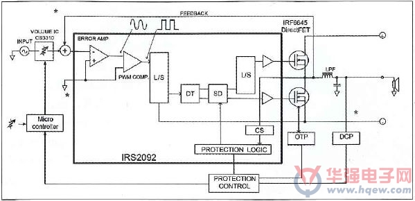
Irs2092 integrates error amplifier, PWM comparator, MOSFET conversion stage with dead time insertion function and overload protection function, which are the main functional components of class D amplifier. The module diagram in Figure 2 describes these functions.

Figure 2: module diagram of irs2092 class D amplifier IC.
The built-in error amplifier is based on the optimized operational amplifier with high noise immunity with a bandwidth of 9MHz, which enables designers to achieve audio distortion (THD) far below 0.01%. Then, the PWM comparator converts the analog signal into PWM with short propagation delay, which allows the designer to freely optimize the feedback loop. Usually, a part of the switching signal is fed back to the input of the error amplifier and preprocessed by low-pass filter. However, the distortion and load dependence can be reduced by shortening the distance between the feedback from the output. Irs2092 enables designers to obtain feedback and increase stability compensation from any point considered to be the best, so as to achieve enthusiast level harmonic distortion and noise (THD + n) performance.
The high voltage level shifter converts the ground reference digital signal into the gate drive signal with each source of the high-end and low-end MOSFET as the reference, so that no matter what the voltage difference at each end is, it can accurately forward the PWM signal, just like the ideal differential amplifier. The patented junction isolation method can prevent the noise generated by the output circuit from interfering with the input signal.
The dead time is inserted between the conduction states of the gate drive stage to prevent the conduction states in the high and low MOSFET at the same time. In fact, irs2092 allows designers to choose the length of dead time according to the selected MOSFET. The guarantee period saves the designer from evaluating the worst case.
Unlike the discrete solution, irs2092 has built-in overload protection, which can monitor the output current and turn off PWM if the predetermined threshold is exceeded.
Other important amplifier features closely related to the design of the power conversion stage include measures to eliminate EMI generated by the pulse width modulator and circuits to reduce switching noise during startup and shutdown. By implementing these features internally, irs2092 further reduces the design overhead and the number of components. This method solves the power electronics design challenges related to class D amplifiers, and lays a foundation for engineers to further improve performance by using professional audio skills.
Actual integrated amplifier
In order to provide further help to the designer, IR proves that this method is also applicable to the 120W double channel half bridge reference design iraudamp5. When using irf6645 directfet MOSFET to drive 2x60W in the 4 Ω speaker load, the amplifier achieves a very low thd+n (0.005%) at the output. Moreover, 96% channel efficiency is achieved at 120W. The reference design can provide guidance for selecting external integrator elements and RC filter elements required in the feedback (from the power output stage) channel. In addition, it also provides all required household power supplies, optimized board layout, PCB manufacturing details and bill of materials. The design can operate normally under 1/8 continuous rated power without radiator, and the output power and the number of channels can be expanded.
Another important aspect of audio amplifier design is to ensure the correctness of startup and shutdown procedures and prevent the transients occurring during these intervals from generating audible switching noise through the output speakers. Traditionally, these transients are excluded from the speakers by inserting a series relay that connects the speakers to the audio amplifier only after initiating transient passage and disconnects the speakers before turning off the amplifier. Because irs2092 integrates the switching noise elimination function, iraudamp5 can disconnect the speaker without any series relay to prevent audible transient noise.
Single package class D amplifier
Using this method, the next level of integration is to add power MOSFET optimized for digital audio applications, PWM controller, gate driver circuit and integrated protection features in the same package. IR‘s latest powiraudio series integrated power modules achieve this goal, allowing designers to further reduce the number of components for high-efficiency amplifiers for high-performance high fidelity audio, home theater systems, car audio and other applications, and reduce the size of the circuit board by as much as 70%.
The four powiraudio devices in this series include ir4301m, ir4311m, ir4302m and ir4312m. They support 35w/4 Ω ~130w/4 Ω full bridge and half bridge topologies, allowing designers to configure 2.1-channel, 5-channel, 6-channel and 7.1-channel applications. These devices have a wide operating voltage range. The operating voltages of ir4301/4302 and ir4311/4312 are as high as 62v/ ± 31v and 32v/ ± 16V respectively. Other important features common to the series include overcurrent protection, thermal shutdown, internal / external shutdown, and floating differential input. Ir4302 and ir4312 also have chip detection function.
Using these devices, designers can build amplifiers for typical music playback applications, which do not need mechanical radiators and can achieve excellent audio performance, such as thd+n as low as 0.02%. The high noise resistance of the controller IC ensures reliable operation under various environmental conditions. These devices are packaged in heat dissipation pqfn, with sizes of 5mm x 6mm (ir4301/4311) and 7mm x 7mm (ir4302/4312), so the advantages of IR advanced class D combined packaging solution are maximized.
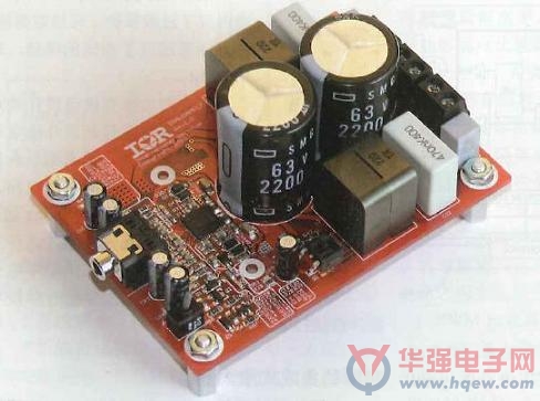
In order to help complete the customized design, a total of 6 reference designs are provided, using ir4301 and ir4302 with single ended and independent power supply configuration, and ir4311 and ir4312 with single ended power supply. These designs are for 35W, 70W, 100W, and 130W applications, including configurations with and without radiators. The reference design of iraudamp17 with ir4302 and 100W dual channel radiator free amplifier is shown in Figure 3.

Figure 3: 100W dual channel class D reference design using ir4302.
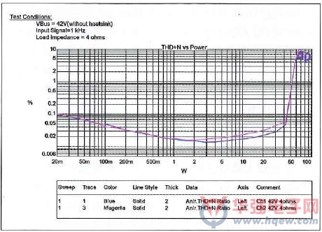
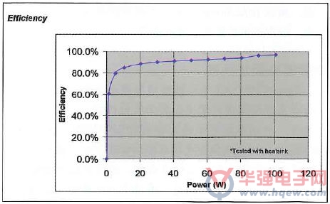
The relationship between amplifier power consumption and thd+n performance is shown in Figure 4, and the relationship between efficiency and power consumption is shown in Figure 5.

Figure 4: relationship between thd+n and power consumption of iraudamp17 reference design using ir4302.

Figure 5: relationship between efficiency and power consumption of iraudamp17 reference design with ir4302.
By simplifying the acquisition method of the new generation of turnkey class D chip amplifiers, these reference designs can help designers overcome the challenge of heat dissipation, achieve miniaturization and set new standards within a wide range of rated audio output power suitable for products such as home cinemas and TVs, audio extensions, active speakers, musical instruments and aftermarket automotive systems.
Using this method, designers can ensure that all projects are completed within a reasonable time window, achieve the specified audio quality goals, and set new standards for product miniaturization and achieve highly competitive prices.
Original statement: this content is originally created by AET website and cannot be reproduced without authorization.
Original statement: this content is originally created by AET website and cannot be reproduced without authorization.
|
Disclaimer: This article is transferred from other platforms and does not represent the views and positions of this site. If there is infringement or objection, please contact us to delete. thank you! |


