A method of heat dissipation management for High Power PCB
Time:2022-07-30
Views:1950
Author: Stefano lovati
The entire power electronics industry, including RF applications and systems involving high-speed signals, is moving towards solutions that provide more and more complex functions in a smaller and smaller space. Designers are facing more and more rigorous challenges in meeting the requirements of system size, weight and power, including effective heat dissipation management, which starts from the design of PCB.
Active power devices with high integration (such as MOSFET transistors) will emit a lot of heat, so PCB is required to transfer heat from the hottest components to the stratum or heat dissipation surface, so as to operate as efficiently as possible. Thermal stress is one of the main causes of power device failure, because it will lead to performance degradation, and may even lead to system failure or failure. The rapid growth of device power density and the continuous improvement of frequency are the main reasons for the overheating of electronic components. Although semiconductors with lower power loss and better thermal conductivity, such as wide band gap materials, have been widely used, they themselves are not enough to eliminate the need for effective heat dissipation management.
At present, the junction temperature of silicon-based power devices is about 125 ℃ and 200 ℃. However, it is best to always let the device work within this limit condition, so as to avoid rapid aging of the device and shorten its remaining life. In fact, it is estimated that if the operating temperature rises by 20 ℃ due to improper heat dissipation management, the remaining life of components will be reduced by as much as 50%.
Layout method
The heat dissipation management method commonly used in many projects is to use the substrate with standard flame retardant grade 4 (FR-4), which is a cheap and easy to process material, focusing on the heat dissipation optimization of circuit layout.
The heat dissipation management method commonly used in many projects is to use the substrate with standard flame retardant grade 4 (FR-4), which is a cheap and easy to process material, focusing on the heat dissipation optimization of circuit layout.
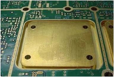
The main measures adopted involve the provision of additional copper surfaces, the use of thicker wiring, and the insertion of heat dissipation holes under components that generate the most heat. A more radical technology that can emit more heat includes inserting real copper blocks into the PCB or applying them to the outermost layer. This copper block is usually in the shape of a coin, so it is named "copper coin". After the copper coin is processed separately, it can be welded or directly attached to the PCB, or it can be inserted into the inner layer and connected with the outer layer through the heat dissipation hole. A special cavity is made in the PCB shown in Figure 1 to hold a copper coin.

Figure 1: PCB with copper coins
The thermal conductivity of copper is 380w/mk, that of aluminum is 225w/mk, and that of FR-4 is 0.3w/mk. Copper is a relatively cheap metal, which has been widely used in PCB manufacturing; Therefore, it is an ideal choice for making copper coins, cooling holes and strata - all of these solutions can improve heat dissipation.
The correct placement of active devices on the circuit board is the key factor to prevent the formation of hot spots, so as to ensure that the heat is evenly distributed on the whole circuit board as much as possible. In this regard, active devices should not be distributed around the PCB in a specific order, so as to avoid the formation of hot spots in specific areas. However, it is best to avoid placing active devices that generate a lot of heat near the edge of the circuit board. On the contrary, they should be placed as close to the center of the circuit board as possible, so as to facilitate uniform heat distribution. If high-power devices are installed near the edge of the circuit board, heat will accumulate at the edge, thereby increasing the local temperature. On the other hand, if it is placed near the center of the circuit board, the heat will be dissipated in all directions along the surface, so that the temperature can be reduced more easily and the heat can be dissipated more easily. Power devices should not be placed close to sensitive components, and should be properly separated from each other.
Measures taken at the layout level can be further improved by using active cooling and passive cooling systems (such as radiators or fans) - such systems can remove heat from active components rather than directly emitting it to the circuit board. Generally speaking, designers must find a suitable compromise between different cooling management strategies according to the requirements of specific applications and available budgets.
PCB substrate selection
Due to its low thermal conductivity (between 0.2 and 0.5w/mk), FR-4 is generally not suitable for applications that need to emit a lot of heat. The heat generated in high-power circuits may be considerable, and these systems often operate in harsh environments and extreme temperatures. Compared with the traditional FR-4, it may be a better choice to use an alternative substrate material with higher thermal conductivity.
For example, ceramic materials provide significant advantages for heat dissipation management of high-power PCB. In addition to improving thermal conductivity, these materials also have excellent mechanical properties, which help to compensate for the stress accumulated during repeated thermal cycles. In addition, ceramic materials have low dielectric loss at frequencies up to 10GHz. For higher frequencies, you can always choose mixed materials (such as PTFE), which can provide the same low loss, but the thermal conductivity will be moderately reduced.
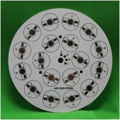
The higher the thermal conductivity of the material, the faster the heat transfer. Therefore, in addition to being lighter than ceramics, metals such as aluminum also provide an excellent solution that can transfer heat from components. In particular, aluminum is also an excellent conductor, with excellent durability, recyclability, and non-toxic. Due to the high thermal conductivity, the metal layer helps to transfer heat quickly on the whole circuit board. Some manufacturers also provide metal clad PCBs, of which two outer layers are metal clad, usually aluminum or galvanized copper. From the perspective of unit weight cost, aluminum is the best choice, while copper has higher thermal conductivity. Aluminum is also widely used to manufacture PCBs that support high-power LEDs (as shown in the example in Figure 2), where its ability to reflect light from the substrate is particularly useful.

Figure 2: example of aluminum PCB for high power RGB LED
Even silver, because its thermal conductivity is about 5% higher than copper, can also be used to make wires, through holes, pads and metal layers. In addition, if the circuit board is used in a humid environment with toxic gases, the use of silver finish on exposed copper wires and copper pads will help prevent corrosion - a typical threat known in such environments.
Metal PCB, also known as insulating metal substrate (IMS), can be directly laminated into PCB to form a board with FR-4 substrate and metal core. The single-layer and double-layer technology is adopted, with deep control wiring, which can transfer heat from on-board components to less important areas. In IMS PCB, a thin layer of conductive but electrically insulated dielectric is laminated between the metal substrate and copper foil. The copper foil is etched into the required circuit pattern, and the metal substrate will absorb heat from the circuit through the thin dielectric.
The main advantages provided by IMS PCB are as follows:
·The heat dissipation is significantly higher than that of the standard FR-4 structure.
·The thermal conductivity of dielectrics is usually 5 to 10 times higher than that of ordinary epoxy glass.
·The efficiency of heat transfer is much higher than that of traditional PCB.
In addition to LED technology (lighting signs, displays and lighting), IMS circuit boards are also widely used in the automotive industry (headlights, engine control and power steering), power electronics (DC power supply, inverter and engine control), switches and semiconductor relays.
|
Disclaimer: This article is transferred from other platforms and does not represent the views and positions of this site. If there is infringement or objection, please contact us to delete. thank you! |


