Six Major Causes of Mosfet Tube Leakage Current
Time:2023-04-16
Views:1567
When discussing MOS transistors, there are basically six leakage current components in short channel devices:
Reverse bias - PN junction leakage current
• Subthreshold leakage current
• Potential barrier reduction caused by drain
• V roll down
• The impact of operating temperature
• Tunnel entry and passage of gate oxide leakage current
Leakage current caused by hot carrier injection into the gate oxide layer from the substrate
• Leakage current caused by gate induced drain reduction (GIDL)
Before continuing, please ensure that you are familiar with the basic concepts of MOS transistors, which will prepare the following information for you.
1. Reverse bias PN junction leakage current
The drain/source and substrate junctions in MOS transistors are reversely biased during transistor operation. This can cause reverse bias leakage current in the device. The leakage current may be due to the drift/diffusion of minority carriers in the reverse bias region and the electron hole pair due to the avalanche effect. The reverse bias leakage current of the PN junction depends on the doping concentration and junction area.
For heavily doped PN junctions in the drain/source and substrate regions, interband tunneling (BTBT) effect dominates the reverse bias leakage current. In interband tunneling, electrons tunnel directly from the valence band in the p-region to the conduction band in the n-region. For electric fields greater than 106 V/cm, BTBT is visible.
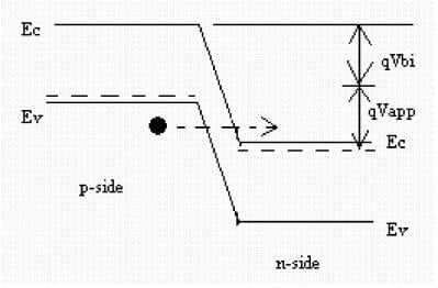


Figure 1 Interband tunneling in reverse biased PN junctions of MOS transistors. All images were provided by K. Roy et al., "Leakage Current Mechanism and Leakage Reduction Techniques in Deep Submicron CMOS Circuits"; Process. IEEE, Volume. 91, Issue 2, February 2003.
Please note that in the context of this article, we define tunneling phenomenon as occurring even when the electron energy is much lower than the potential barrier.
2. Subthreshold leakage current
When the gate voltage is less than the threshold voltage (V th) but greater than zero, the transistor is referred to as biased in the subthreshold or weakly inverted region. In weak inversion, the concentration of minority carriers is small but not zero. In this case, the typical value for | V DS | is>0.1V and the entire voltage drop occurs at the drain substrate pn junction.
When the gate voltage is less than the threshold voltage (V th) but greater than zero, the transistor is referred to as biased in the subthreshold or weakly inverted region. In weak inversion, the concentration of minority carriers is small but not zero. In this case, the typical value for | V DS | is>0.1V and the entire voltage drop occurs at the drain substrate pn junction.
The electric field component parallel to the Si SiO2 interface between the leakage sources is very small. Because of this negligible electric field, the Drift current can be ignored, and the subthreshold current is mainly composed of Diffusion current.
Drain Induced Barrier Reduction (DIBL)
The subthreshold leakage current is mainly caused by the decrease of potential barrier or DIBL caused by the drain. In short channel devices, the interaction between the drain and source depletion regions reduces the potential barrier of the source. Then the source can inject charge carriers into the channel surface, resulting in sub threshold leakage current.
DIBL is evident in high drain voltage and short channel devices.
V roll down
The threshold voltage of MOS devices decreases due to a decrease in channel length. This phenomenon is called Vth rollover (or threshold voltage rollover). In short channel devices, the drain and source depletion regions further enter the channel length, depleting a portion of the channel.
Therefore, a smaller gate voltage is required to reverse the channel, thereby reducing the threshold voltage. This phenomenon is evident for higher drain voltages. The decrease in threshold voltage increases the subthreshold leakage current, as the subthreshold current is inversely proportional to the threshold voltage.
The impact of working temperature
Temperature also has an impact on leakage current. The threshold voltage decreases with increasing temperature. Alternatively, in other words, the subthreshold current increases with increasing temperature.
3. Leakage current of tunneling gate oxide layer
In short channel devices, thin gate oxides generate high electric fields on the SiO 2 layer. The low oxide thickness with high electric field causes electrons to tunnel from the substrate to the gate and from the gate to the substrate through the gate oxide, resulting in gate oxide tunneling current.
Consider the energy band diagram shown in the figure.

Figure 2. Energy band diagram of MOS transistors with (a) flat band, (b) positive gate voltage, and (c) negative gate voltage
Figure 2 (a) shows a flat band MOS transistor, where there is no charge present.
When the gate terminal is positively biased, the energy band diagram will change, as shown in the second figure, Figure 2 (b). The electron tunnel at the strongly reversed surface enters or passes through the SiO 2 layer, resulting in gate current.
On the other hand, when a negative gate voltage is applied, the electron tunnel from the n+polysilicon gate enters or passes through the SiO 2 layer, resulting in gate current, as shown in Figure 2 (c).
Fowler Nordheim Tunnel and Direct Tunnel
There are two main tunneling mechanisms between the gate and substrate. They are:
Fowler Nordheim tunneling effect, where the electron tunnel passes through a triangular barrier
Direct tunneling effect, where the electron tunnel passes through a trapezoidal barrier
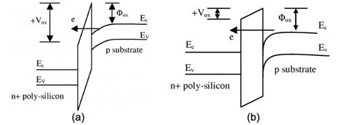

Figure 3 The energy band diagram shows (a) the Fowler Nordheim tunnel passing through the triangular barrier of the oxide, and (b) the trapezoidal barrier of the oxide directly passing through the tunnel
You can see the energy band diagrams of the two tunneling mechanisms in Figures 3 (a) and 3 (b) above.
4. Leakage current caused by hot carrier injection from substrate to gate oxide
In short channel devices, high electric fields near the substrate oxide interface excite electrons or holes, which pass through the substrate oxide interface and enter the oxide layer. This phenomenon is called hot carrier injection.
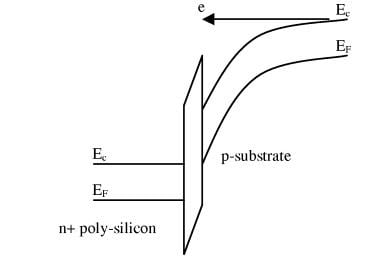
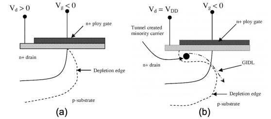

Figure 4 The energy band diagram depicts the electron obtaining sufficient energy due to a high electric field and crossing the peroxide barrier potential (hot carrier injection effect)
This phenomenon is more likely to affect electrons rather than holes. This is because compared with holes, electrons have smaller effective mass and smaller barrier height.
5. Leakage current caused by gate induced drain reduction (GIDL)
Consider NMOS transistors with p-type substrates. When there is a negative voltage at the gate terminal, positive charges accumulate at the oxide substrate interface. Due to the accumulation of holes on the substrate, the surface exhibits a heavier p-region than the substrate doping.
This results in a thinner surface depletion zone along the drain substrate interface (compared to the thickness of the depletion zone in the main body).

Figure 5. (a) A thin depletion zone is formed along the surface of the drain substrate interface, and (b) GIDL current flow caused by the avalanche effect and the carrier generated by BTBT
Due to the thin depletion region and high electric field, avalanche effect and interband tunneling (as described in this part) will occur. Therefore, a few carriers in the drain region below the gate are generated and pushed into the substrate by negative gate voltage. This increases the leakage current.
6. Leakage current caused by through effect
In short channel devices, due to the proximity of the drain terminal and source terminal, the depletion regions of the two terminals will gather together and eventually merge. In this case, it is said that a "breakdown" occurred.
The through effect reduces the potential barrier of most charge carriers from the source. This increases the number of charge carriers entering the substrate. Some of these carriers are collected by the drain electrode, while the remaining carriers cause leakage current.
|
Disclaimer: This article is transferred from other platforms and does not represent the views and positions of this site. If there is any infringement or objection, please contact us to delete it. thank you! |


