The Processing Method of Inductance in PCB Design
Time:2023-06-18
Views:927
Inductors are very common components in electronic circuits, and they can be classified into different types according to different classification methods. They have their own unique roles and characteristics in different application scenarios.

Firstly, the composition of inductance is mainly composed of two parts: winding and magnetic core, specifically including:
1. Winding: Consisting of a conductor coil wound on a magnetic core, usually made of copper or aluminum wire. The cross-sectional area and number of turns of the wire determine the size of the inductance. The winding can be wound in single or multiple layers, or in parallel or cross wires.
2. Magnetic core: It can be made of various materials such as hollow tube, solid magnetic material, or magnetic powder. The material of the magnetic core can affect the performance of the inductor, participate in the transmission of magnetic field, and mainly improve the magnetic flux of the inductor device.
It is worth noting that the internal structure of inductors may vary depending on specific application scenarios and manufacturing processes. For example, the magnetic core of iron core inductors is composed of materials such as iron, nickel, and iron oxide, as well as various types of micro inductors and SMD inductors, all of which have different structures.
In addition, some inductance devices will be equipped with auxiliary components such as anti shaking capacitors and winding protective sleeves to improve circuit efficiency and protect the structure of the inductance.

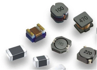
We will talk about the use of one of the commonly used inductors, the power inductor, and its handling methods in our PCB design. Firstly, power inductors can be divided into shielded inductors and unshielded inductors. The biggest difference between the two is that one can see the wound coil, and the other cannot be seen because it is covered by a metal shield. Power inductors are mainly used in power electronic equipment, It is usually one of the core components of circuits such as AC/DC converters, DC/DC converters, filter networks, and regulated power supplies. The functions and functions of power inductor devices are as follows:
1. Filtering: The power inductor assigns an impedance to the load circuit to separate high-frequency and low-frequency signals. The filtering inductor is mainly used for stabilizing power supplies and filtering the output waveform of power supplies, reducing the ripple and pulsation of the power supply.
2. Transient response: the power inductor can conduct Transient response and transition control on the current in the power supply, prevent transient overcurrent and current pulse in the power supply, and improve the stability of the system.
3. Energy storage: In power electronic devices such as AC/DC converters and DC/DC converters, power inductors store energy and convert it into an electric field to provide higher current or voltage in a short period of time.
4. Isolation: Power inductance can provide a means of isolation to isolate the input power supply from the output part, reducing the interactive electrical interference and noise of the cylinder.
In summary, power inductor is one of the key components in power electronic equipment and plays a very important role in many applications, effectively solving problems such as ripple and current overload in circuits.
When designing a PCB, there is a magnetic field generated during the operation of the inductor, which changes over time. If the strength of this magnetic field is large enough, it will cause interference with surrounding electronic devices. This interference may lead to performance degradation of the circuit, signal interference, and other issues.
In order to reduce the interference of inductors on surrounding electronic devices, some copper sheets are usually excavated around the inductors. This is because the magnetic field generated by the inductor is transmitted to the surrounding electronic devices through copper sheets. If we dig out the copper skin, we can reduce the radiation range of the magnetic field, thereby reducing the impact of EMI.
In addition to removing the copper skin, other measures can also be taken to reduce the interference of the inductor on surrounding electronic devices. For example, they can place a shielding cover around the inductor to further reduce the radiation range of the magnetic field. In addition, technologies such as low noise power supplies and ground wires can also be used to reduce the impact of EMI.
In summary, EMI is a very important issue in PCB design. An inductor is a common electronic component that generates a magnetic field that may interfere with surrounding electronic devices. To reduce this interference, some copper skin is usually dug out around the inductor and other measures are taken to reduce the impact of EMI. These measures can help us design more stable and reliable circuit systems.
Of course, inductance has more than just these effects on the circuit. If the copper sheet is not removed, there will be an eddy current between the inductance magnetic field and the copper sheet, which will cause the inductance area to heat up and reduce the inductance. When encountering a PCB with a shielding cover, we also need to pay attention to the treatment of the inductance area. Usually, a hole is dug in the shielding cover area above the power inductor to avoid the occurrence of eddy current phenomenon.
We have learned so much about it above, so in fact, we only need to pay more attention to the layout of the inductance area and the treatment of the copper sheet in PCB design. A reasonable circuit layout can help us reduce the impact of EMI. Alternatively, we can use shielded inductors. Shielded inductors, due to the presence of a shield, can limit the magnetic induction line inside the shield, thereby reducing the impact on surrounding components. The disadvantage is that they are more expensive, so we usually need to consider them comprehensively.
|
Disclaimer: This article is transferred from other platforms and does not represent the views and positions of this site. If there is any infringement or objection, please contact us to delete it. thank you! |


