Analysis on the Mechanism and Suppression Measures of Burst in Class D Power Amplifiers
Time:2023-07-15
Views:845
With the development of electric vehicles, the number of channels and output power of in car audio systems are gradually increasing. In audio and video entertainment systems, a high channel count and high output power audio system can generate greater sound pressure and dynamic range, enhance the sense of enveloping space, and thus achieve 360 degree surround sound for theater effects. In addition to in car entertainment, the in car audio system also has many functions. Compared to traditional internal combustion engine vehicles, electric vehicles are quieter. To protect pedestrians and reduce accidents, all new electric vehicles require an acoustic vehicle alarm system (AVAS) that emits an appropriate sound. In addition, in the emergency call (Ecall) system, the audio system can trigger collision avoidance prompts and vehicle deviation warnings to enable the driver and emergency dispatcher to contact. The audio system includes many parts, including power amplifiers, ADC, Codec, and more, in addition to the speakers. Among them, Class D power amplifiers have emerged in the field of car audio due to their advantages such as high output power, high efficiency, and small size.
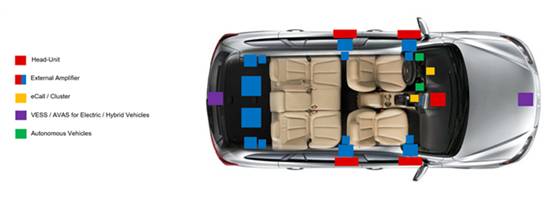
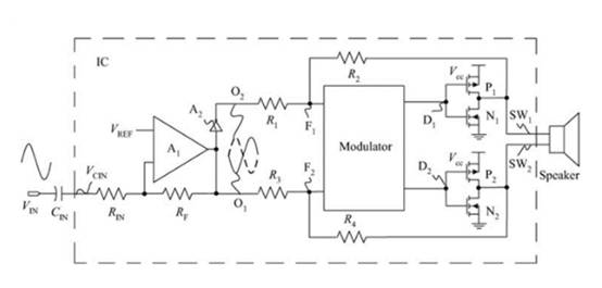

Figure 1. Cockpit Sound System Horn Distribution Diagram
When a digital D-class amplifier is just powered on or when the amplifier‘s playback state is switched, the human ear occasionally hears a "bang" sound, which we call pop noise. There are many reasons for the appearance of pop noise in digital power amplifiers. This article mainly analyzes the reasons for pop noise and provides corresponding solutions.
1) Capacitor charging and discharging

Figure 2. Schematic diagram of single ended power amplifier structure
Figure 2 shows a single ended input power amplifier, while A1 is a comparative amplifier used to set gain and enhance the load capacity of the input signal. The A2 output is completely opposite to the A1 output. The Modulator is used for signal modulation, comparing the input analog signal with a triangular wave to generate a PWM wave to drive the peripheral MOS. One end of the comparison amplifier A1 is directly connected to the reference voltage Vref, and the other end is connected to input audio signals through RIN and CIN connections. When the system is powered on, Vref immediately rises to the reference voltage value, while the other end of A1 needs to be charged to the RIN and CIN for a period of time before it can rise to the reference voltage value. After amplifying the voltage difference between the two ends of A1, the output generates pop noise. In this scenario, the pop noise can be reduced by reducing the input capacitance value, such as switching to 1uf or 0.47uf.
For differential power amplifiers, if the output peripheral hardware circuits of the P and N terminals do not match or the input peripheral hardware circuits do not match, the establishment time of the input signals at both ends of the power amplifier will be different, and the differential signal difference will also be input into the power amplifier and form a pop sound. As shown in the figure below, if the voltage rise speed at both ends of A1 is consistent, the pop noise is 0. A 5ns signal establishment time difference can generate a pop sound that can be heard by the human ear.
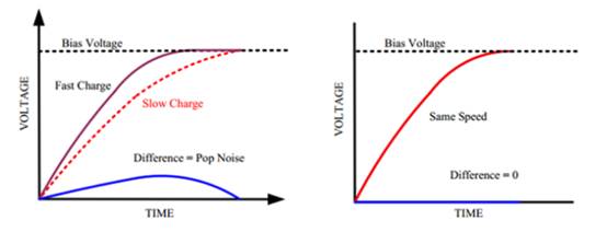
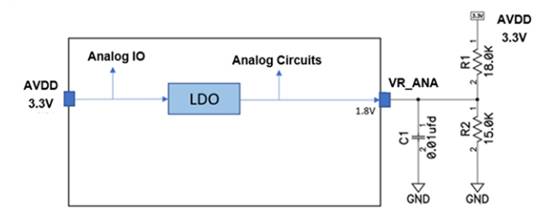
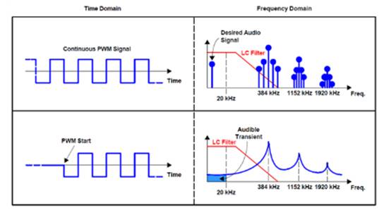
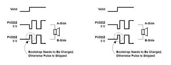
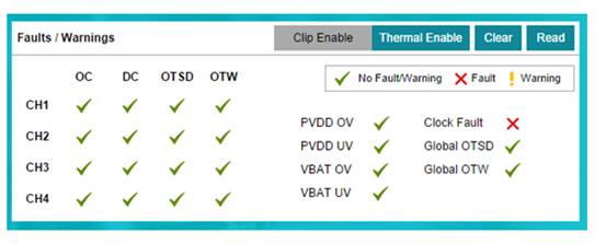

Figure 3 POP Noise at Different Charging Speeds
As shown in Figure 4, VR_ The voltage of ANA is converted from AVDD through LDO, which can cause VR_ The voltage of ANA rises slower than that of AVDD. Here, 1.5V is obtained by dividing the voltage of the AVDD 3.3V resistor, and in VR_ Place a pre bias voltage on ANA to ensure VR_ ANA increases simultaneously with 3.3V, thereby reducing pop noise. Among them, capacitors are used to eliminate 3.3V noise.

Figure 4. POP noise suppression circuit
2) PWM start stop
When the system loses power or is powered on, the playback status of the power amplifier switches, or the input sound source switches, PWM will generate a start stop, thereby generating a transient POP sound. As shown in the figure below, during continuous PWM operation, the switching frequency and its nearby mirror frequency can be smoothly filtered out by the LC filter. When PWM starts and stops, the switching frequency and its odd harmonic will extend to the range of 20-2kHz that can be heard by the human ear. The switching frequency is lower than the cutoff frequency of the LC filter and cannot be filtered out to generate pop tones.

Figure 5. Time frequency domain diagram of continuous PWM and PWM start
When performing AD modulation on the BTL structure power amplifier, PWM activates the first duty cycle. If the A-side is pulled down, the Bootstrap capacitor can charge smoothly, but the B-side is pulled up at this time, which causes the Bootstrap capacitor to fail to charge. The Bootstrap capacitor provides the charging voltage of the N MOSFET. If the Bootstrap capacitor fails to charge, the first PWM on the B-side cannot output normally. The imbalanced output of A-side and B-side will produce a noticeable POP sound. TI has optimized this type of pop noise, making the first PWM low in both AD and BD modulation, thereby eliminating clock faults.

Figure 6 Schematic diagram of AD modulation PWM activation
3) Power on/off sequence error
The audio system has a strict power on/off sequence. Usually, the power supply voltage of the power amplifier is higher than that of the SOC, and it is also established earlier than the SOC voltage. To avoid pop noise during SOC power on and amplifier power on, it is necessary to keep the amplifier in the Hi zi/standby state and wait for the amplifier to fully charge (20ms) before turning on the PWM wave and inputting the sound source. Similarly, when the power amplifier is powered off, in order to avoid inconsistent power down speed, we need to Mute and lower the Standby pin by 15ms before proceeding with power down. TI‘s PurePath Digital has an optimized startup sequence, which minimizes the pop of audible audio tapes.
4) PVDD voltage/Gain value rapidly increases
A sharp increase in PVDD voltage or a rapid increase in Gain value can lead to pop noise. When drawing the schematic diagram, it is necessary to set the Cstart soft start capacitor within a reasonable range to prevent PVDD from rapidly rising. In addition, for some amplifiers, a second pop noise occurs after the first pop noise when turned on. This is because after the power amplifier is powered on, the gain value will climb up to the set gain in a certain step size. If the step size setting value is too large, it will cause pop noise to appear.
5) Hizi play state switch Clock Fault
If the speaker not only produces a pop sound during startup or state transition, but also continuously produces a pop noise when the amplifier switches from Hi zi to play, it should be checked to see if a Clock Fault occurs. Hardware engineers can disconnect the IIC control of the SOC and connect the IIC to PPC3 through a USB adapter for Clock Fault verification.

If a Clock Fault occurs at this time, check whether the input audio signal I2S/TDM meets the requirements of the data manual (see Serial Audio Port in the Electrical Characteristics section of the data manual). In addition, there are other special situations explained in the data manual. Taking the TAS6424L/M-Q1 series as an example, if the customer connects SCLK and MCLK together, FSYNC needs to be at least 2 MCLK. If the SOC is Qualcomm 8155 series, there are three options for FYSNC output: the first is 2MCLK, the second is 50% duty cycle, and the third is 1 slot. We can choose the last two options as FSYNC inputs.
Texas Instruments TAS6424E-Q1 is a four channel digital input class D audio amplifier with 2.1MHz switching frequency. In terms of cost, the operating frequency of the chip is 2.1MHz, which allows the chip to use smaller and lower cost LC filters, thereby achieving overall cost optimization. While increasing the switching frequency, the TI TAS6424E-Q1 chip exhibits good EMI performance through frequency spreading and PWM sequence optimization. In addition, the chip integrates AC and DC fault diagnosis, which can achieve fault diagnosis such as load short circuit to power supply, load short circuit to ground, load open circuit, load short circuit, and achieve high-precision load impedance and phase measurement. In addition, the TAS6424E-Q1 chip integrates optimization of power-on startup sequence and the first PWM solution for low-level suppression of pop sound, achieving a good user listening experience. In addition to low pop noise, the Burr Brown audio architecture and increased internal audio loop bandwidth of the chip can also provide excellent audio quality, bringing a good user experience.
|
Disclaimer: This article is transferred from other platforms and does not represent the views and positions of this site. If there is any infringement or objection, please contact us to delete it. thank you! |


