Schematic diagram and PCB design considerations of three-phase non-inductive DC brushless motor chip ACM6753
Time:2023-11-22
Views:559
summary
ACM6753 is a 5V-18V, three-phase non-inductive BLDC (Brushless DC) motor drive IC, 180 ˚ Sine, integrated drive algorithm+pre drive+MOS, built-in current detection.
Precautions for schematic design

Precautions:
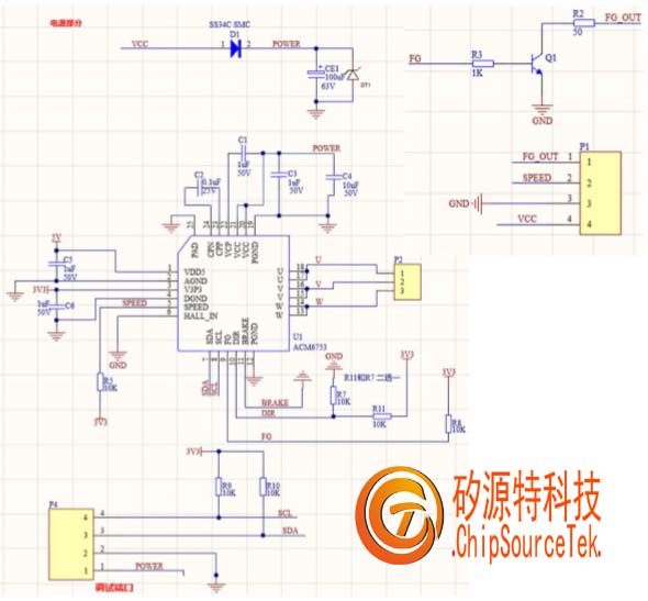
1 Try to leave a pull-up resistor (R5 in the figure) for the SPEED pin, so that the chip does not immediately enter low-power mode after power on. If there is no pull-up resistor and the front PWM is grounded, the chip will enter low-power mode. If it is the I2C mode control chip speed regulation, it is necessary to pull up the SPEED pin. If it is a fixed parameter burning method, it is not necessary to pull up the SPEED pin. To save area, it can be omitted.
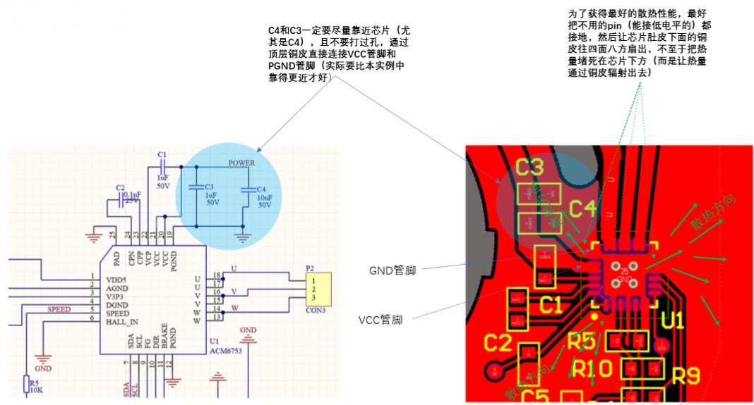
2. Be sure to have a 10uF capacitor close to the VCC pin (pin20/pin21) and GND pin.
3. The DIR pin is used as the highest priority to control the direction of motor rotation. It is recommended to design a compatible pull-up or pull-down resistor for the DIR pin in the early stages of the project when the U/V/W three-phase wire sequence is uncertain (but only one resistor can be welded during welding, as shown in the figure where only one resistor can be welded for R7 and R11)
If you want to burn the program on the board, SCL and SDA must have a resistor pulled up to 3.3V. If the chip is burned and written before mounting, SCL and SDA can not be pulled up or even grounded (for the convenience of fanning out the copper sheet), and suspension is not allowed.
5. HALL_ The IN pin, DIR pin, and BRAKE pin cannot be suspended. FG can be suspended without use.
6. Debugging/burning port (P4) is for the convenience of burning (5V can be directly used with USB), and 5V can be directly connected to VCC pin as the burning voltage. Of course, if the chip is burned well before mounting, this seat is not needed.
7. The withstand voltage of the FG pin is 5V. Note that the output of ACM6753 is open drain, and the FG pin needs to be pulled up to 3.3V or 5V. If the external FG voltage is>5V, a triple joint Q1 needs to be added for isolation The collector output terminal of Q1 serves as the final output of FG. The output of the transistor Q1 is connected to a resistor R2, which should not be too large, otherwise FG_ The low level of the OUT signal cannot be sufficiently low. FG_ OUT must have a pull-up resistor pulled up to external high voltage, and communicate well with the customer (or their customer)
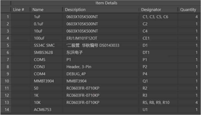
BOM list (for reference only, can be simplified according to specific projects in practice)


BOM simplification:
1) If FG is not required, the FG pin of ACM6753 can be suspended
2) If the chip is burned before mounting. SCL and SDA pins can be directly grounded.
3) If the direction has been determined, the DIR pin can even be directly grounded.
4) If the brake is not used, the BRAKE pin can be directly grounded.
5) HALL_ The IN pin is generally not used and is directly grounded.
5) HALL_ The IN pin is generally not used and is directly grounded.
6) If the power is not high (for example, for applications within 12V/10W, the total capacitance on VCCs of 47uF or less is usually sufficient)
PCB layout

For detailed product information and sales contact information, please refer to: //m.sipemd.com/
|
Disclaimer: This article is transferred from other platforms and does not represent the views and positions of this site. If there is any infringement or objection, please contact us to delete it. thank you! |


