abstract
This article will introduce a reference design for the power architecture of analog true wireless stereo (TWS) earphone applications. It can increase the fast charging speed of applications by nearly four times, while optimizing solution size and system BOM costs. The test results obtained using thermistors and thermal imaging measurements show lower temperatures compared to traditional solutions. This design demonstrates the numerous advantages offered by a solution that utilizes a single inductor, multiple output (SIMO) architecture and has automatic margin tracking capabilities.
introduction
With the continuous advancement of wearable device innovation, the demand for a robust power architecture continues to increase. In the past decade, we have seen a significant growth in wearable health monitoring devices, and the next generation of these devices may integrate more features in the same small-sized solution. Wearable devices typically require support for Wi Fi, Bluetooth ® And it has vital sign monitoring (VSM) function. The demand for more functions requires system level and IC level designers to choose wearable device power architecture more wisely.
The Power Challenge of Wireless Earphones
The application of true wireless stereo headphones currently requires multiple independent regulators to be placed in a small size solution - after all, the entire system needs to be placed in our pockets!
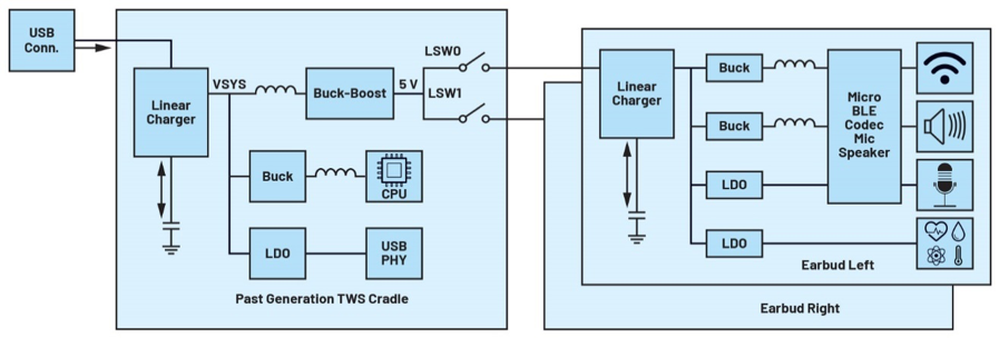
The typical power system for TWS earphone applications is shown in Figure 1a. The DC-DC converter between the charging stand and the headphones is used to increase the voltage from VSYS to 5 V USB level. This can provide sufficient margin for the linear charger of the earphones, avoiding voltage drops. However, this solution has a drawback, which is the significant efficiency loss due to the pressure difference and loss on the linear charging FET of the earphones. This is particularly noticeable when the battery level of the headphones is low. Inefficient charging can increase heat generation, leading to shortened battery life and reduced product reliability.
In some cases (Figure 1b), adding power line communication (PLC) and utilizing the step-down regulator on the charging dock side to track the margin of the linear charger can improve system efficiency.
However, the solution size of wearable products is very valuable. The PLC chips and inductors required to power the step-down output of wearable devices‘ peripherals will directly affect the product size and cost of these two traditional solutions.
Better solution: SIMO architecture and automatic margin tracking
SIMO Power Management IC (PMIC) provides the architecture and efficiency required to meet compact design requirements. Battery-powered wearable applications can also benefit from a technology called automatic margin tracking, which can fully reduce the voltage drop on the battery charging circuit and provide optimization margin to adjust the charging current. This reduces power loss and heat generation in the charging circuit without the need for additional components, allowing wearable devices to maintain lower temperatures during charging and even charge faster.
Figure 1a Typical power architecture diagram for TWS earphone application
Figure 1b. Typical power architecture diagram of TWS earphone application with PLC
MAX77659 is a SIMO PMIC designed to improve the efficiency of wearable consumer and medical devices, while reducing system board space and BOM size. This PMIC has three buck boost outputs using the same inductor, with an efficiency of up to 90%. It also includes an additional Low Voltage Difference (LDO) regulator, suitable for sensitive applications that require high Power Supply Voltage Rejection Ratio (PSRR), such as VSM. In addition, the SIMO architecture has inherent advantages in efficiency, and its static current is very low, resulting in a very small solution size.
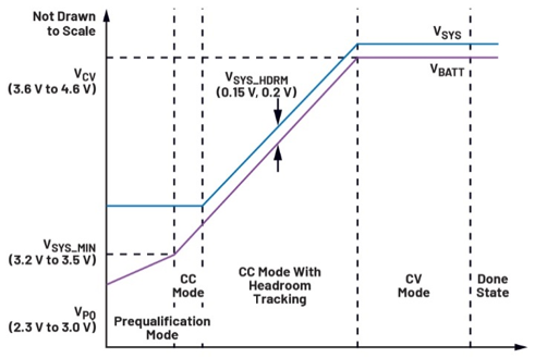
Figure 2. Automatic margin tracking for typical lithium-ion battery charging cycles
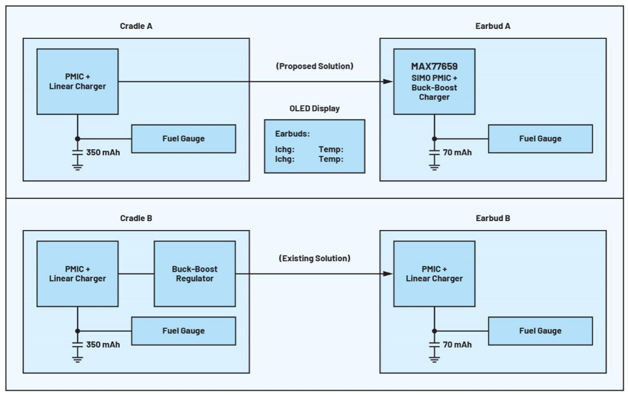
Figure 3. Referring to the design block diagram, a comparison was made between the proposed solution and the traditional solution for TWS earphones
The automatic margin tracking function of MAX77659 uses one of the SIMO outputs to fully reduce the voltage drop on the battery charging transistor, while providing optimized margin to adjust the charging current. The result is a reduction in power loss and heat generation on the transistor, all of which do not require additional components. Figure 2 shows the automatic margin tracking during the entire fast charging process.
MAX77659 reference design
The reference design shown in Figure 3 compares the MAX77659 SIMO PMIC solution with a typical linear charging solution. The MAX77659 SIMO PMIC has an automatic margin tracking function, which eliminates the use of step-down voltage regulators in traditional solutions (Figure 3, charging dock B). It improves charging efficiency, extends the battery life of the entire system, reduces solution size, and lowers BOM costs.
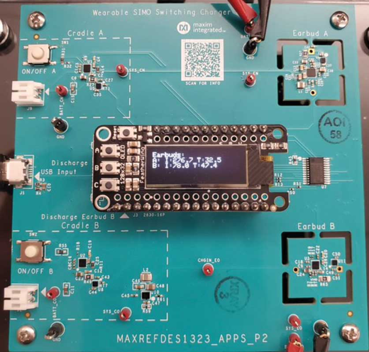
Figure 4. MAXREFDES1323 Reference Design Board
Figure 4 shows the complete PCB of the MAX77659 reference design. This design includes two pairs of charging stand/headphone solutions, one using the MAX77659 SIMO PMIC design (charging stand/headphone A), and the other using a typical linear charger design (charging stand/headphone B), using the MAX77734 linear charger. The buttons on the substrate can switch the charging of branches A and B, and the OLED display screen displays the charging current and temperature measured by the MAX17260 battery meter of the earphones. The screen also displays the status of the charger and when the charger must reduce the charging current due to overheating.
Charging standards for battery management systems
The Japan Electronics and Information Technology Industry Association (JEITA) has released standards related to battery management systems, which provide strict and robust methods to improve system safety and reliability by reducing system and battery wear, providing assurance for end-users. Terminal applications typically utilize integrated JEITA protection functions to reduce charging current and voltage levels during the constant current (CC) and constant voltage (CV) stages of battery charging. If the system becomes too hot, the charging current and voltage can be reduced to cool down the circuit. This limitation on current can protect end-users from discomfort and maintain the reliability and lifespan of the system. Unfortunately, limiting the charging current also means that the charging cycle slows down. The requirement to integrate JEITA functionality represents a design trade-off, which puts pressure on wearable device design. A solution that can maintain good thermal performance even by receiving high charging current for a long time can alleviate this pressure.
performance comparison
To test the thermal performance of both traditional and proposed solutions, we conducted a 270 mA CHG_ CC (normal CC current) and 75 mA JEITA_ A 1-minute charging test was conducted at CC (CC current above the JEITA_WARM temperature threshold). The goal is to display the thermal difference during this period and check if both solutions can maintain a high charging speed without triggering JEITA protection. In order to provide repeatability and limit the temperature rise to only the temperature rise experienced by the IC, we used a battery simulator. The thermal threshold used in this test is 45 ° C, which is 21 ° C higher than the ambient temperature. The reference design PCB is a 6-layer board with copper thicknesses of 0.0014 inches, 0.0007 inches, 0.0007 inches, 0.0007 inches, and 0.0014 inches, respectively. The test conditions are shown in Table 1, and the results are shown in Table 2.
Table 1. JEITA Charging Test Conditions
|
Test Configuration
|
|
CC
CC
|
270 mA
270 mA
|
|
JEITA CC
JEITA CC
|
75 mA
75 mA
|
|
JEITA Warm
JEITA
Warm temperature
|
45˚C
45˚C
|
|
Batt Voltage
battery voltage
|
3.0 V
3.0 V
|
Table 2. JEITA Charging Test Results
|
Solution A (MAX77659 SIMO PMIC)
|
Solution B (Linear Charger))
|
|
Time (s)
(s)
|
Status
|
Temp (˚C)
(°C)
|
Charge
Current
(mA)
(mA)
|
Status
|
Temp (˚C)
(°C)
|
Charge
Current
(mA)
(mA)
|
|
0
0
|
Off
|
24.3
24.3
|
270
270
|
Off
关
|
24.0
24.0
|
270
270
|
|
15
15
|
CC
CC
|
29.1
29.1
|
270
270
|
CC
CC
|
43.0
43.0
|
270
270
|
|
30
30
|
CC
CC
|
32.2
32.2
|
270
270
|
JEITA CC
JEITA CC
|
47.1
47.1
|
75
75
|
|
45
45
|
CC
CC
|
33.3
33.3
|
270
270
|
JEITA CC
JEITA CC
|
47.3
47.3
|
75
75
|
|
60
60
|
CC
CC
|
35.4
35.4
|
270
270
|
JEITA CC
JEITA CC
|
44.2
44.2
|
75
75
|
During the testing process, the MAX77659 SIMO solution heated up 11.1 ° C within 1 minute and its heating rate significantly slowed down after the first 30 seconds. The proposed solution did not enter JEITA mode at any time during the testing process. When using a typical linear charging solution, the device heats up to 20 ° C in just 15 seconds and triggers JEITA protection, limiting the charging current in just 30 seconds.
Thermal imaging results
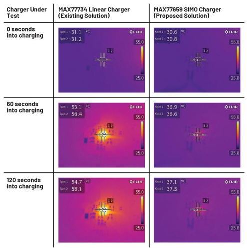
In addition, to check thermal behavior without enabling JEITA protection, we conducted separate tests and used a thermal imager to measure the temperature of the SIMO PMIC solution and linear charger solution. The parameters are the same as the first test, except that JEITA protection is disabled.
Figure 5. Thermal imaging of parallel charger solution
During the 2-minute testing process, the temperature of the linear solution rose to 58.1 ° C, while the SIMO PMIC only rose to 37.5 ° C. Based on these results, it can be concluded that compared to linear charging solutions, SIMO solutions can reduce temperature rise and fall by about 72%.
conclusion
This article compares the MAX77659 SIMO PMIC with traditional linear charging solutions in simulating TWS earplug applications, demonstrating the advantages of automatic margin tracking and switch charger solutions. The results indicate that the SIMO PMIC solution has achieved significant thermal improvements (72% reduction in heat) and can safely maintain almost four times the charging current of traditional linear charging solutions. This helps the system to charge quickly while maintaining low temperature and comfort, thus solving the key challenges of wearable devices.
MAX77659 SIMO PMIC provides a safe, reliable, and comfortable charging solution for the next generation of wearable devices, while improving efficiency and reducing the necessary solution size and system BOM quantity. For more information, please visit ADI‘s comprehensive SIMO PMIC and battery meter platform to view excellent low-power solutions for next-generation wearable devices.
|
Disclaimer: This article is transferred from other platforms and does not represent the views and positions of this site. If there is any infringement or objection, please contact us to delete it. thank you!
BD手机网页版官方登录入口-半岛彩票官方网站
ChipSourceTek
|
