How does a boost chip increase voltage
Time:2024-03-07
Views:258
Boost and buck generally refer to the working mode of the power circuit, and some power ICs can support both boost and buck modes simultaneously.

The voltage reduction mode - Bust mode, which is familiar to everyone and widely used, such as 5V ->3.3V voltage stabilization, has many corresponding chips that you can search online, including LDO mode and DC-DC mode. The peripheral circuit of the LDO mode chip is relatively simple, and only filtering capacitors need to be added to the input and output terminals.
The chip circuit in DC-DC mode is relatively more complex, but has higher efficiency. Generally, external capacitors and inductors are required. The inductor is charged by closing the switch, and after disconnecting the switch, the inductor is discharged as a power source. The output voltage value can be adjusted by the PWM duty cycle, and the maximum voltage value will not exceed the power supply voltage.
Boost mode - Boost mode, which is also common and a type of DC-DC. When the entire circuit only uses a single power source (such as a 3.7V lithium battery) for power supply, lower voltages such as 3.3V and 1.6V can be output to power the IC by reducing voltage. Sometimes higher voltages are needed in the circuit, such as driving screens of some mobile devices with higher voltages, such as 12V. It is not practical to add an independent power source of 12 in mobile devices, and lithium batteries are generally 3.7V (fully charged to 4.2V), At this point, it is necessary to use a boost circuit, which also has corresponding ICs. Generally, it needs to be combined with inductors and capacitors to achieve different DC-DC connection methods in boost and buck modes.
By closing the switch to charge the inductor, and disconnecting the switch, the electromotive force of the inductor is connected in series with the power supply, increasing the voltage. The output voltage can be adjusted by the duty cycle of PWM. When the duty cycle is 50%, the output voltage is twice the input voltage.
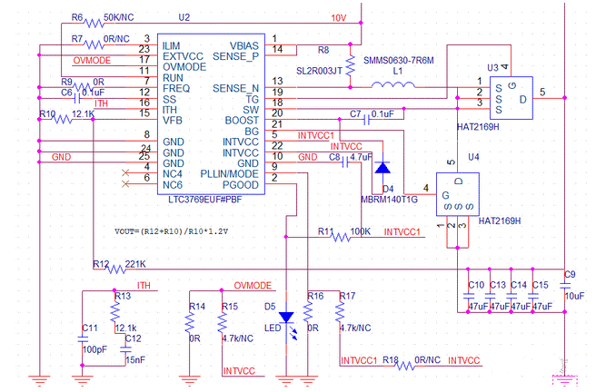
The circuit diagram introduced in this article is an input DC 5V to 10V, output 24V@5A . Working frequency 350KHz (FREQ pin grounded). Burst Mode (PLLIN/MODE pin grounded). As shown in Figure 1

The Boost Converter increases the input voltage to the desired output voltage by changing the working cycle of the circuit. Its working principle is as follows:
1. The input voltage is transmitted to the inductor through a switching transistor (such as MOSFET), causing a current to be generated in the inductor.
2.When the switch tube is closed, the current in the inductor continues to flow, resulting in the generation of magnetic field energy storage.
3. Subsequently, when the switch tube is opened again, the energy stored in the inductor is released, the magnetic field collapses, and a reverse voltage is generated.
4. This reverse voltage will help increase the output voltage, making it higher than the input voltage.
5. By controlling the switching cycle and duty cycle of the switching tube, the output voltage can be adjusted to achieve voltage boosting operation.
The boost chip utilizes a combination of inductors and switching tubes to periodically store and release energy, in order to increase the output voltage and achieve voltage boost.
|
Disclaimer: This article is transferred from other platforms and does not represent the views and positions of this site. If there is any infringement or objection, please contact us to delete it. thank you! |


