Usage of analog switches
Time:2024-03-24
Views:218
Analog switch definition
Analog switches are mainly used to switch signals in the signal link. The use of MOSFET switching method to turn off or turn on the signal link is achieved, and due to its function similar to a switch, it is implemented using the characteristics of analog devices, which is called an analog switch. Simulated switch circuits can achieve high turn off impedance, usually above megaohms, which is one of the functions of analog switches. To increase everyone‘s understanding of analog switches, this article will introduce the functions of analog switches and the selection methods of analog switches.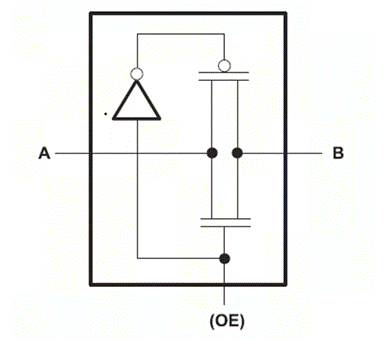
ure 2 Schematic diagram of transmission door switch
Figure 2 shows the schematic diagram of the FET (transmission gate) at the NO/NC port, consisting of an N-channel transistor and a parallel P-channel transistor. When the OE input is high, after passing through the inverter, the P-channel conducts, the N-channel conducts, and A to B conduct. On the contrary, when the OE output is low, the P channel and N channel are blocked, and A to B are turned off.
How to choose analog switches
he main function of analog switches is to switch signals. At present, integrated analog electronic switches have become the dominant product in the small signal field. Compared with traditional mechanical contact electronic switches, integrated electronic switches have many advantages, such as fast switching speed, no jitter, low power consumption, small size, reliable operation, and easy control. But there are also several drawbacks, such as high conduction resistance, limited input current capacity, and small dynamic range. Therefore, integrated analog switches are mainly used in situations where high-speed switching and small system volume are required. Aiwei‘s analog switches are made using CMOS technology and can be applied over a wide frequency range.
When selecting analog switches, the following indicators need to be considered:
1. Number of channels
Integrated analog switches typically include multiple channels. The number of channels has a direct impact on the accuracy of signal transmission and switch switching rate. The more channels there are, the larger the parasitic capacitance. Because when the selected channel is connected, other blocked channels are not completely disconnected, but in a high resistance state with leakage current. In addition, there is coupling and parasitic capacitance between channels, so there is mutual interference between channels.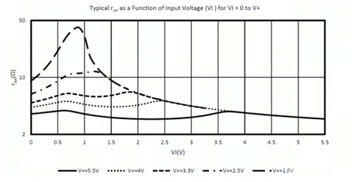
Figure 3 Relationship between Ron and VIN
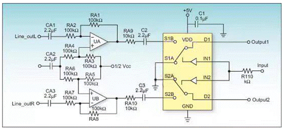
Figure 4 Audio front-end amplification and signal gating circuit
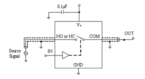
Figure 5 Analog Switch Equivalent Circuit
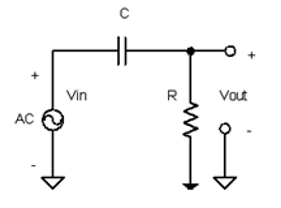
Figure 6 Equivalent circuit when the analog switch is disconnected


Analog switches are mainly used to switch signals in the signal link. The use of MOSFET switching method to turn off or turn on the signal link is achieved, and due to its function similar to a switch, it is implemented using the characteristics of analog devices, which is called an analog switch. Simulated switch circuits can achieve high turn off impedance, usually above megaohms, which is one of the functions of analog switches. To increase everyone‘s understanding of analog switches, this article will introduce the functions of analog switches and the selection methods of analog switches.
operational principle
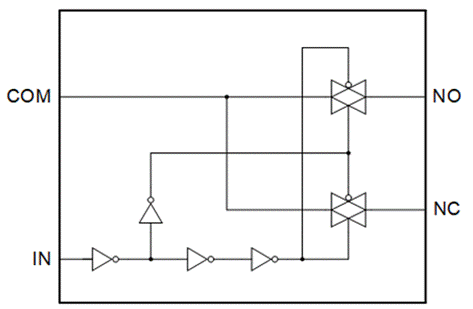
Figure 1: Working principle of analog switch
The working principle of the analog switch is shown in Figure 1. When the input at the IN end is low, the channel between COM and NC is closed through logical control, and the channel between COM and NO is opened. When the input at the IN end is high, it is the opposite.

Figure 1: Working principle of analog switch

ure 2 Schematic diagram of transmission door switch
How to choose analog switches
he main function of analog switches is to switch signals. At present, integrated analog electronic switches have become the dominant product in the small signal field. Compared with traditional mechanical contact electronic switches, integrated electronic switches have many advantages, such as fast switching speed, no jitter, low power consumption, small size, reliable operation, and easy control. But there are also several drawbacks, such as high conduction resistance, limited input current capacity, and small dynamic range. Therefore, integrated analog switches are mainly used in situations where high-speed switching and small system volume are required. Aiwei‘s analog switches are made using CMOS technology and can be applied over a wide frequency range.
When selecting analog switches, the following indicators need to be considered:
1. Number of channels
Integrated analog switches typically include multiple channels. The number of channels has a direct impact on the accuracy of signal transmission and switch switching rate. The more channels there are, the larger the parasitic capacitance. Because when the selected channel is connected, other blocked channels are not completely disconnected, but in a high resistance state with leakage current. In addition, there is coupling and parasitic capacitance between channels, so there is mutual interference between channels.
2. Leakage current
An ideal switch requires zero resistance when conducting, infinite resistance when disconnecting, and zero leakage current. When the actual switch is disconnected, it is in a high resistance state and the leakage current is not zero. The conventional CMOS leakage current is about 1nA. If the internal resistance of the signal source is high and the transmitted signal is a current, it is particularly necessary to consider the leakage current of the analog switch. Generally, the smaller the leakage current, the better.
3. Conduction resistance
The flatness of the conducting resistance is consistent with the conducting resistance. Conducting a resistor will result in signal loss, leading to a decrease in accuracy, especially when the load connected in series with the switch is of low impedance and the loss is greater. In application, switches with sufficiently low conduction resistance should be selected according to the actual situation. It must be noted that the value of the conducting resistance is directly related to the power supply voltage. Generally, the larger the power supply voltage, the smaller the conducting resistance, and the conducting resistance and leakage current are contradictory. If a small conducting resistance is required, the channel should be expanded, which will result in an increase in leakage current. The conducting resistance fluctuates with the variation of input voltage, and the flatness of the conducting resistance refers to the maximum fluctuation value of the conducting resistance within the limited input voltage range Δ RON= Δ RONMAX - Δ RONMIN. It indicates the flatness of the conducting resistance, Δ The smaller the RON, the better. The consistency of the conduction resistance represents the difference in the conduction resistance of each channel. The better the consistency of the conduction resistance, the smaller the error caused by the switch when the system collects various signals.
4. Switching speed
The speed at which a switch is turned on or off. Usually represented by the on time TON and off time TOFF. For situations where fast changing signals need to be transmitted, it is required to have a high switching speed of the analog switch, while also considering adapting to the speed of the subsequent sampling and holding circuit and A/D converter, in order to select the device with the best performance to price ratio.
5. Switching withstand voltage
Analog switches, due to their application in low-voltage working environments of electronic boards, generally have a withstand voltage value of less than 15V. Common maximum withstand voltage values include 3.3V, 5V, 12V, 15V, etc. When selecting, attention must be paid to the maximum voltage of the signal link and the maximum withstand voltage value of the device.
6. THD (Total Harmonic Distortion)
This indicator can measure the fidelity of analog switches to audio signals. Some audio signal processing requires strict THD, which is defined as the dB ratio of signal power to harmonics and noise. The flatness of the conducting resistance of THD and analog switches is related. Generally speaking, as the conduction impedance increases, the flatness of the conduction impedance (i.e. the variation of the conduction impedance within the input voltage range) also increases accordingly. The increase in the flatness of the conduction impedance will decrease the THD performance. That is to say, the flatter the conduction impedance within the input voltage range, the better the THD performance.
Analog switch applications
Analog switches are different from mechanical switches, and their semiconductor characteristics need to be considered when using them:
1. The on resistance (Ron) varies with the input signal (VIN)

Figure 3 Relationship between Ron and VIN
2. Injecting charges
e certainly hope that the lower the Ron, the better when using mechanical switches, because low resistance can reduce signal loss. However, for analog switches, low Ron is not suitable for all applications. A lower Ron requires a larger chip area, resulting in larger input capacitance. During each switching cycle, its charging and discharging processes consume more current. The time constant t=RC, and the charging time depends on the load resistance (R) and capacitance (C), usually lasting for several tens of nanoseconds. This indicates that low Ron has longer on and off times. Therefore, the selection of analog switches should comprehensively balance Ron and injected charges.
3. Switching withstand voltage
When the input signal is too low (below zero potential) or too high (above power supply voltage), the MOSFET is in reverse bias. When the voltage reaches a certain value (exceeding the limit of 0.3V), the switch cannot function properly or even be damaged. Therefore, in the application of analog switches, it is important to note that the input signal must not exceed the specified range.
Figure 4 shows the front-end amplification and signal selection circuit of a sound equipment, which uses a four channel operational amplifier and a dual channel analog switch

Figure 4 Audio front-end amplification and signal gating circuit
The original intention of this scheme design is to gate the Lineouts L and Lineouts R audio signals when Input=0. When Input=1, the PhoneoutL and PhoneoutR audio signals are gated. However, when the experimental machine was made, it was found that when Input=1, a considerable portion of the signals from Lineouts L and Lineouts R channels were leaked to the D1 and D2 terminals, respectively. Using a network analyzer to test the turn off isolation of the analog switch, when the input signal is 10kHz, the turn off isolation of the switch is -120dB, so the chip should not have any problems.
In fact, the circuit has the following two errors in analog switch applications:
1. The input signal of the analog switch is missing a DC bias
The circuit of the analog switch can be equivalent to Figure 5. The minimum input signal of the analog switch in CMOS technology can only reach -0.3V. If it is further below this value, the chip will not function properly and may even be damaged. The input signal of the analog switch in Figure 4 does not have a DC bias, so a part of the input signal is in the negative value range, and the analog switch naturally cannot work properly.

Figure 5 Analog Switch Equivalent Circuit
Solution: Remove both capacitors C2 and C3, and the analog switch input signal will have a DC bias signal of 1/2VDC. At this time, the analog switch can work from rail to rail.
2. Lack of coupling resistance at D1 and D2 ends
When the analog switch is disconnected, its input and output terminals are equivalently connected in series with a capacitor C. If it is assumed that there is an equivalent resistance R between the output terminal of the analog switch and ground, the equivalent circuit of the analog switch when disconnected is shown in Figure 6.

Figure 6 Equivalent circuit when the analog switch is disconnected
At this point, the analog switch is actually equivalent to an RC filtering circuit, and it is not difficult to derive the following formula:

Among them, Uout is the analog switch output signal, Uin is the analog switch input signal, R is the analog switch output terminal resistance load, C is the equivalent capacitance when the analog switch is disconnected, and f is the input signal frequency.
Due to the design of the equivalent capacitance C of the analog switch being very small, when the input signal f is in the audio region, the gain A is determined by both R and f. When the value of R is small, f plays a dominant role, and at this time, A<<1, the signal is effectively isolated. When the value of R is large, R plays a dominant role. At this point, A ->1, and the signal is almost completely leaked. So when the output terminal is suspended, the resistance between its output terminal and ground R ->+∞, and the analog switch is fully conductive at this time.
After correcting the above two errors, the audio application circuit can now function properly. From the above examples, it can be seen that fully understanding the basic concept of analog switches is the basis for correctly applying analog switches.
Introduction to AW Analog Switch
Aiwei Electronics is committed to providing customers with better solutions and offers the following analog switch products to choose from:

Among them, AW35301STR is a single path single pole double throw analog switch with a conducting resistance of 3 Ω and a bandwidth of 400MHz. It is packaged in SOT363-6L and can be used for audio routing, selection, chopping, modulation and demodulation applications.
AW35321QNR adopts a green and environmentally friendly small volume QFN 1.8mm * 1.4mm * 0.55mm – 10L packaging. The ultra-low conductivity resistance of 0.5 Ω (typical value) and the ability to support negative swing signals with only a single power supply make it very suitable for application in the audio field. This package has a small footprint and is very suitable for compact electronic devices such as mobile phones, PADs, and ultrathin laptops.
AW35321QNR adopts a green and environmentally friendly small volume QFN 1.8mm * 1.4mm * 0.55mm – 10L packaging. The ultra-low conductivity resistance of 0.5 Ω (typical value) and the ability to support negative swing signals with only a single power supply make it very suitable for application in the audio field. This package has a small footprint and is very suitable for compact electronic devices such as mobile phones, PADs, and ultrathin laptops.
|
Disclaimer: This article is transferred from other platforms and does not represent the views and positions of this site. If there is any infringement or objection, please contact us to delete it. thank you! |


