CST2466/CT2466E概述:
CST2466/CST2466E 为电池供电的玩具、低压或者电池供电的运动控制应用提供了一种集成的有刷直流马达驱动解决方案。
CST2466/CST2466E 电路内部集成了采用 N 沟和 P 沟功率 MOSFET 设计的 H 桥驱动电路,适合于驱动有刷直流马达或者驱动步进马达的一个绕组。
CST2466/CST2466E 电路具备较宽的工作电压范围(从 2V 到 11V), 最大持续输出电流达到 2.1A(ESOP),最大峰值输出电流达到 3.5A。该驱动电路内置过热保护电路。通过驱动电路的负载电流远大于电路的最大持续电流时,受封装散热能力限制,电路内部芯片的结温将会迅速升高,一旦超过设定值 (典型值 150℃), 内部电路将立即关断输出功率管,切断负载电流,避免温度持续升高造成塑料封装冒烟、起火等安全隐患。内置的温度迟滞电路,确保电路恢复到安全温度后,才允许重新对电路进行控制。
CST2466/CST2466E 提供SOP8和ESOP-8封装形式。
The CST2466/CST2466E provides an integrated motor driver for cameras, consumer products, toys and other application with low-voltage or battery-powered motion control.
The CST2466/CST2466E can supply up to 2.1A of output DC current. It operates on a motor power supply (VM) from 2 to 11V and a device power supply voltage (VCC) of 2V to 6V. Ultra- low RDS-ON allows SOP-8 package available.
The CST2466/CST2466E has a PWM (INA、INB) input interface. Full protections are integrated with over-current protection, under-voltage lockout and over-temperature shutdown.
CST2466/CT2466E特性:
CST2466/CT2466E ABSOLUTE MAXIMUM RATINGS
CST2466/CT2466E RECOMMENDED OPERATING CONDITIONS(Ta=25℃)
Note:The maximum continuous output current depends on the heat dissipation conditions. 2.1A(ESOP8) 1.68A(SOP8)
CST2466/CT2466E ELECTRICAL CHARACTERISTICS
(Ta=25℃,VCC=3V,VM=6V,unless otherwise specified )
CST2466/CT2466E INPUT AND OUTPUT TRUTH TABLE
CST2466/CST2466E 为电池供电的玩具、低压或者电池供电的运动控制应用提供了一种集成的有刷直流马达驱动解决方案。
CST2466/CST2466E 电路内部集成了采用 N 沟和 P 沟功率 MOSFET 设计的 H 桥驱动电路,适合于驱动有刷直流马达或者驱动步进马达的一个绕组。
CST2466/CST2466E 电路具备较宽的工作电压范围(从 2V 到 11V), 最大持续输出电流达到 2.1A(ESOP),最大峰值输出电流达到 3.5A。该驱动电路内置过热保护电路。通过驱动电路的负载电流远大于电路的最大持续电流时,受封装散热能力限制,电路内部芯片的结温将会迅速升高,一旦超过设定值 (典型值 150℃), 内部电路将立即关断输出功率管,切断负载电流,避免温度持续升高造成塑料封装冒烟、起火等安全隐患。内置的温度迟滞电路,确保电路恢复到安全温度后,才允许重新对电路进行控制。
CST2466/CST2466E 提供SOP8和ESOP-8封装形式。
The CST2466/CST2466E provides an integrated motor driver for cameras, consumer products, toys and other application with low-voltage or battery-powered motion control.
The CST2466/CST2466E can supply up to 2.1A of output DC current. It operates on a motor power supply (VM) from 2 to 11V and a device power supply voltage (VCC) of 2V to 6V. Ultra- low RDS-ON allows SOP-8 package available.
The CST2466/CST2466E has a PWM (INA、INB) input interface. Full protections are integrated with over-current protection, under-voltage lockout and over-temperature shutdown.
CST2466/CT2466E特性:
单通道内置功率 MOS 全桥驱动
最大连续输出电流可达 2.1A,峰值 3.5A
驱动前进、后退、停止及刹车功能
无需外围滤波电容
内置迟滞热效应过热保护功能
低导通电阻 260mΩ
CST2466/CST2466E提供SOP8和ESOP-8封装形式
H-Bridge Motor Driver
DC Motor or Other Loads
Low On-Resistance :280mΩ
2.1-A Maximum DC Drive Current
Separate Motor and Logic Supply
Motor VM : 2 to 11V
Logic VCC : 2V to 6V
Low-Stand-by Current ≤ 2uA/VM=VCC=5V
Small Package and Footprint
8-Pin ESOP with Thermal PAD
8-Pin SOPProtection Features
VCC Under-voltage Lockout
Over-Current Protection
Thermal Shutdown
CST2466/CT2466E应用
CST2466/CT2466E APPLICATION:
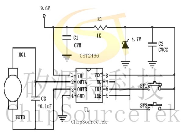
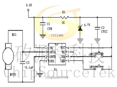
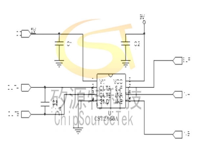
注:如图在 3V 应用中建议 CVM 电容至少用一个 0.1uF;在 4.5V 应用中至少用一个 1uF;在 6V 应用中至少用一个 4.7uF;在 9V 应用中至少用一个 22uF。均为使用贴片电容靠近 IC 之 VDD 管脚放置且电容的负极和 IC 的 GND端之间的连线也需尽量短。即不要电容虽然近,但布线、走线却绕得很远。当使用大电解插件电容时,建议再并一个 0.1uF 贴片电容于 CST2466/CST2466E 之 VM 脚上。 参考下图。
The capacitor C1 connected between the GND and the VM pins must be located as close as possible to the CST2466/CST2466E chip. In different applications, C1(show as above) is recommended to use a 0.1uF in 3V applications; a 1uF is recommended for 4.5V applications; a 4.7uF is recommended for 6V applications; in 9.6V applications, it is recommended to use 22uF, all these capacitors should be SMD package. The connection between the negative pole of the capacitor and the GND terminal of the IC should be as short as possible. That is to say, the line route should not far away.
When the application board has capacitors while filtering for other chips that is far away from the CST2466/CST2466E, it need to place a small capacitor for CST2466/CST2466E.
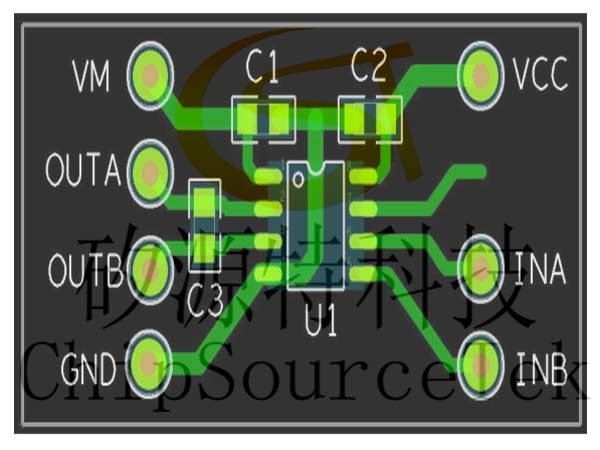
The capacitor C3 preferably soldering to the motor poles instead of placing it on the PCB. When it is inconvenient to soldering on the motor poles, it can be mount on the PCB. The following diagram is the PCB layout reference .

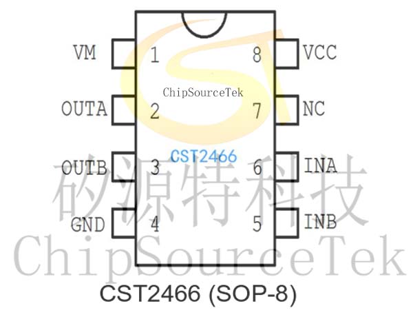
CST2466/CT2466E SOP8脚位图:
CST2466/CT2466E SOP8 PIN DESCRIPTION:
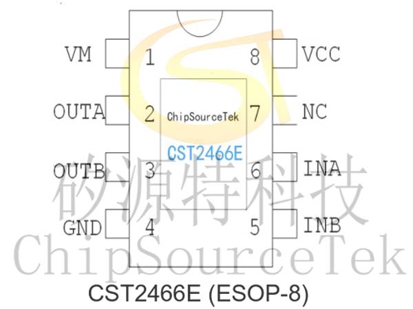
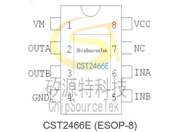
CST2466/CT2466E eSOP8脚位图:
CST2466/CT2466E eSOP8 PIN DESCRIPTION:
CST2466/CT2466E脚位定义:
CST2466/CT2466E Definition of foot position:
H-Bridge Motor Driver
DC Motor or Other Loads
Low On-Resistance :280mΩ
2.1-A Maximum DC Drive Current
Separate Motor and Logic Supply
Motor VM : 2 to 11V
Logic VCC : 2V to 6V
Low-Stand-by Current ≤ 2uA/VM=VCC=5V
Small Package and Footprint
8-Pin ESOP with Thermal PAD
8-Pin SOPProtection Features
VCC Under-voltage Lockout
Over-Current Protection
Thermal Shutdown
CST2466/CT2466E应用
CST2466/CT2466E APPLICATION:
电动牙刷
玩具马达驱动
相机、单反相机镜头驱动
电子锁
机器人
有刷驱动器应用
Electric toothbrush, Electric lock
Cameras
DSLR Lenses
Consumer Products
Toys
Robotics
CST2466/CT2466E PCB布局指导及典型应用电路图:
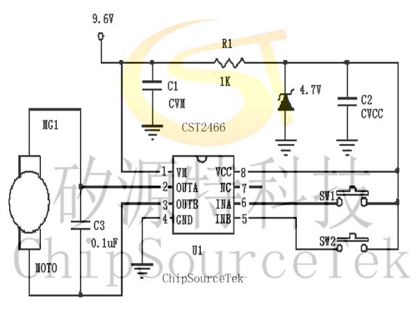
CST2466/CT2466E PCB LAYOUT GUIDANCE
Cameras
DSLR Lenses
Consumer Products
Toys
Robotics
CST2466/CT2466E PCB布局指导及典型应用电路图:

CST2466/CT2466E PCB LAYOUT GUIDANCE
注:如图在 3V 应用中建议 CVM 电容至少用一个 0.1uF;在 4.5V 应用中至少用一个 1uF;在 6V 应用中至少用一个 4.7uF;在 9V 应用中至少用一个 22uF。均为使用贴片电容靠近 IC 之 VDD 管脚放置且电容的负极和 IC 的 GND端之间的连线也需尽量短。即不要电容虽然近,但布线、走线却绕得很远。当使用大电解插件电容时,建议再并一个 0.1uF 贴片电容于 CST2466/CST2466E 之 VM 脚上。 参考下图。
The capacitor C1 connected between the GND and the VM pins must be located as close as possible to the CST2466/CST2466E chip. In different applications, C1(show as above) is recommended to use a 0.1uF in 3V applications; a 1uF is recommended for 4.5V applications; a 4.7uF is recommended for 6V applications; in 9.6V applications, it is recommended to use 22uF, all these capacitors should be SMD package. The connection between the negative pole of the capacitor and the GND terminal of the IC should be as short as possible. That is to say, the line route should not far away.
When the application board has capacitors while filtering for other chips that is far away from the CST2466/CST2466E, it need to place a small capacitor for CST2466/CST2466E.
The capacitor C3 preferably soldering to the motor poles instead of placing it on the PCB. When it is inconvenient to soldering on the motor poles, it can be mount on the PCB. The following diagram is the PCB layout reference .

CST2466/CT2466E SOP8脚位图:
CST2466/CT2466E SOP8 PIN DESCRIPTION:

CST2466/CT2466E eSOP8脚位图:
CST2466/CT2466E eSOP8 PIN DESCRIPTION:

CST2466/CT2466E脚位定义:
CST2466/CT2466E Definition of foot position:
| Pin number | Pin name | I/O | Description |
| 1 | VM | -- | Motor power supply |
| 2 | OUTA | O | Motor drive output A |
| 3 | OUTB | O | Motor drive output B |
| 4 | GND | -- | Ground |
| 5 | INB | I | Logic input B |
| 6 | INA | I | Logic input A |
| 7 | NC | -- | No connection |
| 8 | VCC | -- | Logic power supply |
CST2466/CT2466E ABSOLUTE MAXIMUM RATINGS
| Parameters | Symbol | Value | Unit | |
| Logic power supply voltage , VCC | VCC | 7 | V | |
| Motor power supply voltage , VM | VM | 11 | V | |
| Power dissipation | Pd | SOP-8 | 0.96 | W |
| Operating Temperature, Top | Topr | -20~85 | ℃ | |
| Junction temperature | Tj | 150 | ℃ | |
| Storage Temperature, Tstg | Tstg | -55~150 | ℃ | |
| Manual welding temperature | 350~370 | ℃ | ||
| Peak output current | Iop | 3.5 | A | |
| Continuous Output Current | Ioc | 2.1 | A | |
| PWM Frequency | fPWM | 33 | KHz | |
CST2466/CT2466E RECOMMENDED OPERATING CONDITIONS(Ta=25℃)
| Parameter | Symbol | Rating | Unit |
| Power supply voltage | VCC | 2.0~6 | V |
| Motor Power supply voltage | VM | 9.6 | V |
| High Input Voltage | VIN | 0.5xVCC | V |
| Low Input Voltage | VIN | -0.8~0 | V |
| Continuous Output Current | IOUT | -1500~1500 | mA |
CST2466/CT2466E ELECTRICAL CHARACTERISTICS
(Ta=25℃,VCC=3V,VM=6V,unless otherwise specified )
| Parameter | Symbol | Test Condition | Min | Typ | Max | Unit |
| Overall Circuit | ||||||
| Standby Current | ICCST | INA=INB=GND | — | 1 | 5 | uA |
| Input control | ||||||
| High Input Voltage | VINH | 2 | 4 | 6 | V | |
| Low Input Voltage | VINL | — | — | 0.8 | V | |
| PWM Drive Frequency | FPWM | — | 20 | 33 | KHz | |
| Reverse brake Time Required | RVBT | from INA to INB or from INB to INA |
200 | 500 | — | uS |
| High Input Current | IINH | VIN=3V | — | 250 | 400 | uA |
| Low Input Current | IINL | VIN=0V | -1 | 0 | — | uA |
| Pull Down Resistor | RIN | — | 12 | — | KΩ | |
| Driving | ||||||
| Output Impedance(HS+LS) | RON | Io=±200mA | — | 0.26 | 0.6 | Ω |
| Protection Circuits | ||||||
| Thermal shutdown temperature | TTSD | Die temperature | — | 150 | — | ℃ |
CST2466/CT2466E INPUT AND OUTPUT TRUTH TABLE
| Input | Output | Function | ||
| INA | INB | OUTA | OUTB | |
| L | L | Hi-Z | Hi-Z | Stand-by(Stop) |
| H | L | H | L | A CH output |
| L | H | L | H | B CH output |
| H | H | L | L | Brake |


