Fast DC charging of electric vehicles, common system topologies and power devices
Time:2023-11-26
Views:528
The role of direct current fast charging (DCFC) in eliminating barriers to electric vehicle adoption is evident. The demand for shorter charging time has driven nearly 400 kilowatts of high-power electric vehicle fast charging into the market. This blog will discuss the typical topology of power converters and an overview of power devices for AC-DC and DC-DC used in DCFC.
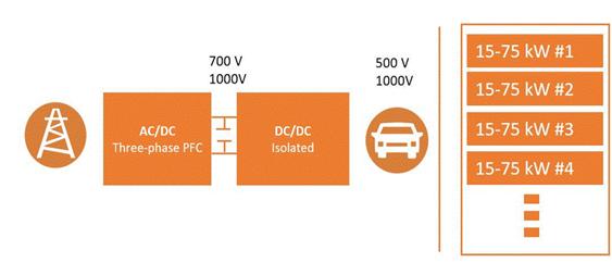
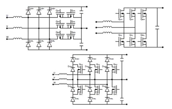
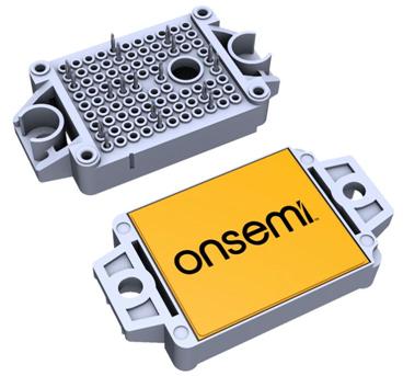
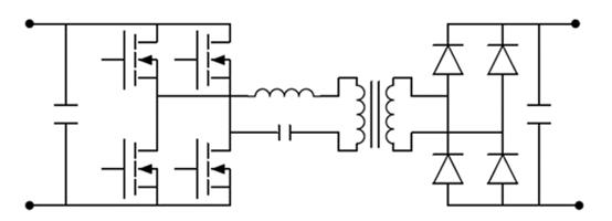
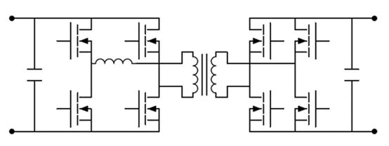
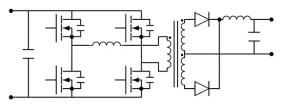
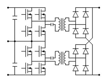

Figure 1. Architecture diagram of DC fast charging for electric vehicles
Active rectification three-phase PFC boost topology structure
Three phase power factor correction (PFC) systems (also known as active rectification or active front-end systems) are receiving increasing attention, and demand has grown rapidly in recent years. The PFC topology is crucial for efficiently supplying power to DCFC. Incorporating silicon carbide (SiC) power semiconductors into your PFC topology can solve challenges, reduce power loss, and increase power density.
The front-end PFC boost stage can be implemented using multiple topologies, and these topologies can meet the same power requirements. Figure 2 shows the common PFC architecture in DCFC applications. One primary difference between them is their bidirectional nature. T-Neutral Clamp (T-NPC) and I-NPC topologies are suitable for bidirectional operation by replacing some diodes with switches. The structure of 6 switches is a bidirectional perse.

Figure 2. Typical PFC boost topology for DCFC T-NPC (top left), 6-switch (top right), and I-NPC (bottom)
Another important factor that affects the design and rated voltage of power devices is the number of stages in the architecture. The topology of 6 switches is a two-level architecture, typically using switches of 900 V or 1200 V to achieve fast DC electric vehicle chargers. The SiC MOSFET module here has the preferred solution for low RDS on (6-40 mQ) regions, especially for high power ranges above 15 kW per block.
This integration demonstrates superior power performance compared to discrete solutions, improves energy efficiency, simplifies design, reduces the size of the entire system, and maximizes reliability. T-Neutral Point Clamp (T-NPC) is a three-level topology structure that uses a 1200 V rectifier (replaced by switches in a bidirectional form), with 650 V switches back-to-back on the neutral path. I-NPC is a 3-level architecture that may be fully implemented with a 650 V switch. 650 V SiC MOSFETs or IGBTs with co packaged diodes represent excellent alternatives to these three-level topologies.

Figure 3. F1-2 PACK SiC MOSFET half bridge module. 1200 V, 10 m Ω
DC-DC topology structure
When studying the DC-DC conversion stage, three isolation topologies were mainly used: full bridge LLC resonant converter (LLC converter), full bridge phase shifted dual active bridge (DAB) zero voltage transition (ZVT) converter (DAB-ZVT converter), and full bridge phase shifted zero voltage transition converter (ZVT converter) (Figures 4, 5, and 6).
Full bridge LLC resonance
The LLC converter achieves zero voltage switching (ZVS) in the primary end and zero current switching (ZCS) in the secondary end at resonant frequencies and below, resulting in very high peak efficiency near the resonant frequency. As a pure frequency modulation (FM) system, when the operating point of the system deviates from the resonant frequency, this may be a situation that requires wide output voltage operation, and the energy efficiency of LLC will decrease. However, advanced hybrid modulation schemes combine pulse modulation (PWM) with frequency modulation today, limiting maximum frequency loss and high loss. However, these hybrid implementation methods still add complexity to the already cumbersome LLC control algorithms. Furthermore, current sharing and synchronization of parallel LLC converters are not an easy task. Generally speaking, LLC is a design that is difficult to surpass when it is possible to operate within a relatively small voltage range and/or when there is development skills to implement advanced control strategies that combine frequency modulation and PWM. It not only provides the highest energy efficiency, but also is a very comprehensive solution from various perspectives. LLC can be implemented as a bidirectional CLLC, which is another complex topology structure.

Figure 4. Full bridge LLC converter
Full bridge phase shifted dual active bridge (DAB) zero voltage transition (ZVT) converter
The DAB-ZVT converter with a secondary synchronous rectification topology is also very typical. These are all operated using PWM, generally requiring simpler control than LLC converters. DAB can be considered as an evolution of traditional full bridge phase-shifting ZVT converters, but the leakage inductor is located at the primary end, which simplifies the tedious secondary end rectification and reduces the necessary rated breakdown voltage of secondary switches or diodes. Due to the implementation of ZVT, these converters can provide stable high energy efficiency over a wide range of output voltages. This is a convenient factor for chargers that support battery voltage levels of 800 V and 400 V. The PWM operation of DAB brings benefits. Firstly, it tends to make the electromagnetic interference (EMI) spectrum of the converter more compact than in frequency modulation systems. In addition, with a fixed switching frequency, the behavior of the system under low loads is easier to solve. Through synchronous rectification, DAB is a bidirectional native topology and is one of the most common alternative and suitable solutions for fast electric vehicle chargers.

Figure 5. Full bridge phase-shifting DAB ZVT converter
Full bridge phase-shift ZVT converter
For unidirectional operation, the traditional full bridge phase shifted ZVT (Figure 6) is still an available option, but the permeability is decreasing. This topology works similar to DAB, but the inductor located at the secondary end brings a significant difference in rectification. The inductor sets a high reverse voltage on the diode, which is proportional and inversely proportional to the duty cycle. Therefore, depending on the operating conditions, the reverse voltage on the diode may exceed the output voltage by two to three times. This situation can be challenging in high output voltage systems, such as electric vehicle chargers, where multiple secondary windings (with lower output voltage) are typically connected in series. This configuration is not very convenient, especially if considering the rated values of power and voltage, different topologies with a single output will provide the same or better performance.
The SiC module represents a very suitable and common solution for the full bridge in the DC-DC power conversion stage mentioned above, with a power higher than 15 kW. Higher frequencies help to reduce the size of transformers and inductors, thereby reducing the overall size of the solution.

Figure 6. Full bridge phase-shift ZVT converter
Variations of topological structure
The discussed topology has multiple variants, bringing additional advantages and compromises. Figure 16 shows a common alternative to a full bridge LLC converter for fast electric vehicle charging. In phase shifting, the switch is below half of the input voltage and uses power off voltage devices of 600 V and 650 V. 650 V SiC MOSFET, 650 V SuperFET 3 Fast Recovery (FR) MOSFET, and 650 V FS4 IGBT will help address different system requirements. Similarly, diodes and rectifiers used for initial extremes require a blocking voltage level of 650 V. These three-level architectures allow for single pole switching, which helps reduce peak current and current ripple, resulting in the use of smaller transformers. One of the main drawbacks of this topology is that the control algorithm requires additional complexity compared to the Level 2 version with fewer power switches. Dual active bridges and dual active bridges can be easily connected in parallel or stacked at the primary and secondary ends to best match the current and voltage requirements of fast electric vehicle chargers.

Figure 7.3- Stage Full Bridge LLC Converter - This variant is stacked at the primary end (only half of the input voltage is applied to each transformer) and connected in parallel at the secondary end
Secondary terminal rectification
Regarding the secondary terminal rectification, as shown in Figure 8, there can be multiple solutions, all of which can use different topologies. For horizontal and full bridge rectification of 400V and 800V batteries, SiC Schottky diodes at 650V and 1200V are typically a unique cost-effective solution. Due to their zero reverse recovery characteristics, these devices greatly enhance rectification performance and energy efficiency compared to silicon-based alternatives, greatly reducing losses and complexity of rectification stages. Silicon based diodes, such as Hyperfast, UltraFast, and Stealth, can serve as substitutes for very limited cost projects, but at the cost of sacrificing performance and increasing complexity. The solution of using center tap rectification (Figure 6) is not convenient for high voltage output rectifier stages. Unlike full bridge rectification, in full bridge rectification, the standard reverse voltage of the diode is equal to the output voltage, while in center tap configuration, the diode has to withstand twice this value. A conventional full bridge phase-shifting converter (with inductance at the secondary end), as explained, requires a higher breakdown voltage diode in both rectification methods (full bridge or center tap rectification). In order to overcome the demand of conventional full bridge phase-shifting converters for 1200 V or 1700 V rated diodes, several outputs will be connected in series.
|
Disclaimer: This article is transferred from other platforms and does not represent the views and positions of this site. If there is any infringement or objection, please contact us to delete it. thank you! |


