TR16F096A(B) General Description:
The TxP16E2TM is a high performance 16-bit MCU, running up to 32MHz and provided with 96K FLASH and total 6K SRAM for high performance process of audio algorithm, power control and motor control. It is the new generation computational kernel for Flash DSP series2. It has initially aimed at the areas of controller and multimedia digital signal processing (DSP) application to demonstrate its profession. TxP16E2 furnish with fast MAC architecture, which allows multiplication+accumulation instructions to be issued with access memory simultaneously during one cycles. The TR16F096A(B) is equipped with TxP16E2 and integrating input/output ports,Audio PWM, Timer and Low Voltage Reset...etc on a chip. Built-in high-speed 12-bit ADC can apply to voice recording application easily.
Furthermore, TR16F096A(B) extend its external device connection capability such as Serial ROM/Flash. The internal memory capacity includes 96Kx16 program/data FLASH plus 6Kx16 working SRAM.
TR16F096A(B) Features:
*Notice: TR16F096A(B) do not support ultra-deep sleep.
*Notice: PortC0 are forbidden to be connected with VCC or pull-up resistance.
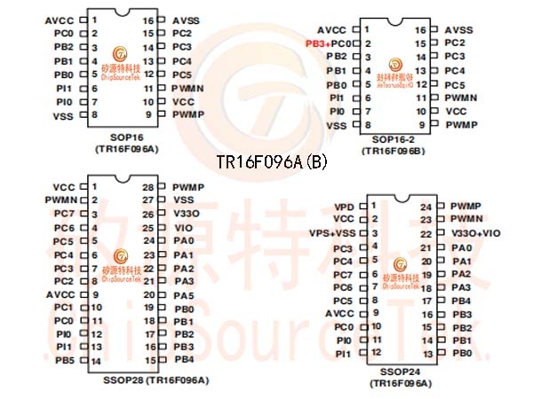
*Notice: TR16F096B only supports SOP16-2 package. (PIN2 is PB3+PC0)
*Notice: TR16F096A(B) does not support buzzer and speaker wake up, so MISC2 bit5, MISC2 bit 6 and MISC3 bit3 should be set to 0.
*Notice: If Microphone is used, OPA1 and OPA2 need to be disable.
*High-performance RISC TxP16E2 CPU
-high working performance 32MIPS@SRAM PM
-Max speed 24MIPS in no branch condition (Turbo-Speed ON) @Flash PM
-Max speed 16MIPS (Turbo-Speed OFF) @Flash PM
-wide working voltage 1.8Volt ~ 5.5Volt
-Operation frequency is programmable by Software
-Built-in 4096x16 SRAM + 2048 x16 SRAM
-Embedded PC Stack Level 24
*Rich DSP function
-Hardware Circular Buffer support
-MAC Computation power : 32 MIPS (max.)
-Multi-Function Support: In MAC calculation, simultaneously access two operands from memory in one cycle
-Extend Dynamic Range: A 40-bit accumulator to ensure in 512 successive multiple+additions no overflows
*Embedded Flash 96Kx16
-Typical 2,0000 erase/program cycles
-Greater than 10 years Data Retention
*Software-based audio processing technical
-Voice recognition, Subband , ADPCM , Melody
*Support 22+2(ICE PAD can be as I/O) general purpose I/O port.
*Stereo 16bit PWM and Mono 16bit DAC
*15 IRQ & 1 FIRQ
-FIRQ can interrupt IRQ immediately
-2 external interrupt
*SPI Master interface with 4 buffers
*SPI Slaver
*UART for IAP(In Application Programming)
*I2C interface
*Three timers: Timer1, Timer2, RTC timer
*Support Spread Spectrum clocking to reduce EMI.
*Watch dog timer (WDT)
*Low voltage reset (LVR)
*Low dropout regulator(LDO) supply 3.3V/2.4V/1.8V@20mA (voltage drop 0.1v)
*PB0, PB1, PB2, PB3 support two edge modes for wake-up function are rising and falling edge trigger.
*Three Comparators
*12bit SAR ADC 12bit / 8 channel
*16bitΣ-Δ ADC
*Microphone with AGC(Auto Gain Control)
*Crystal 32768
*Low voltage detector
*Touch with BG Pre-Charge
*IR 38K
*1402 interface
*PIR / CDS / OPA
*Four I/O pins support de-bounce input
*PortA5 support high sink current 60mA@3.3V
*Notice: Special I/O PortC0 will cause LED flashing light when power on.
*Notice: PortC0 / PortC2 / PortC3 / PortC4 / PortC5 / PortC6 / PortC7 are forbidden to be directly connected to inductive components. For example, motors and coils, etc.
*Notice: VCC Decoupling Cap 10uF should be close to IC within 0.5cm in PCB layout.
*Notice: VCC Decoupling Cap 0.1uF should be close to IC within 0.5cm in PCB layout.
*Notice: The width of VCC and VSS power line should be greater than 30 mil in PCB layout.
*Notice: TR16F096A(B) does not support the function of deep sleep.
TR16F096A(B) Application Field:
*MCU Application
*Electronic Dictionary
*Handheld Games
*Electronic Learning Aid (ELA)
*Electronics storybook
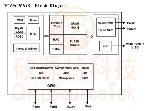
TR16F096A(B) Block Diagram:

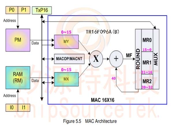
TR16F096A(B) MAC (16-bit X 16-bit Multiplier and Accumulator):
A 16 bit x 16 bit MAC is provided for digital signal processing. The core of MAC operation is multiply MX&MY
with 2’S complement operand and accumulation previous 40-bit MF then rounding store result in the 40-bit MR
register. The basic MAC architecture is shown as Figure 5.5.

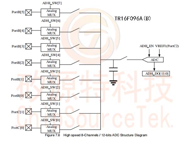
TR16F096A(B) High speed 8-Channels / 12-bits ADC Structure Diagram:

Note: If user need more precise ADC for application, user can set “ADC vref input” to enable VREFI at option. If ADC Verf input is
enabled, PortC2 must be connected 20~100ohm resistor to VCC and 47uF capacitor to AVSS.
Note: Enable ADC verf input at option, PortC2 is as ADC voltage-reference input (VREFI), not as I/O pin.
TR16F096A(B) Touch Controller Structure:

TR16F096A(B) De-bounce Input Source:

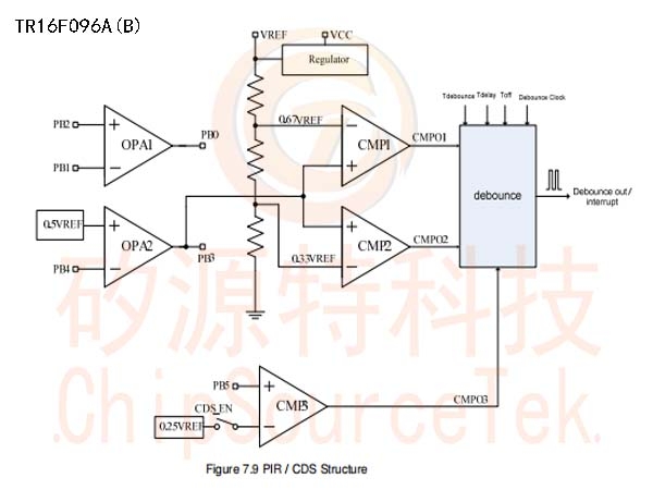
TR16F096A(B) PIR / CDS Structure:

Notice: OPA1 and OPA2 will be low power operation in PIR mode. So the external resistor of OPA should
use high impedance resistor (above 1M ohm).
Notice: If PIR_EN (bit0 of MISC6) is enable, OPA1 and OPA2 will be enabled automatically.
Caution : OPA1_EN (bit2 of MISC6) and OPA2_EN (bit3 of MISC6) must be set to “0” in PIR MODE.
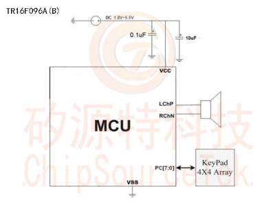
TR16F096A(B) Application Circuit:
Application Circuit: Mono16-bit PWM output
Notice:
1. VCC Decoupling Cap 10uF should be close to IC within 0.5cm in PCB layout.
2. VCC Decoupling Cap 0.1uF should be close to IC within 0.5cm in PCB layout.
3. The width of VCC and VSS power line should be greater than 30 mil in PCB layout.
4. VSS and AVSS are as close as possible.

TR16F096A(B) Package: SOP16 / SOP16-2 / SSOP24 / SSOP28:


